Note:
1. 2Mbps is measured in the 802.11n mode, the MCS =7, the GI = 200uS.
2. Up to + 21.5dBm output powerin 11b mode.
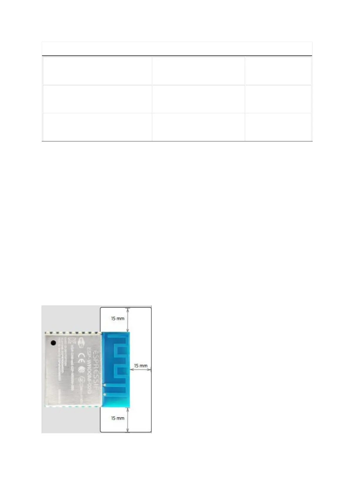
6.PCB Design
Precautions for PCB layout and module layout:
1. Pay attention to the placement of the module during PCB layout, especially the antenna
part of the module, as far as possible away from interference sources: magnetic
components (such as motors,inductance, transformers, etc.), high-frequency signal
devices (such as crystal oscillators, high-frequency clock signals, etc.).
2. The upper and lower layers of the PCB where the module is placed should not be routed
as much as possible. Do the copper-clad processing, and the PCB from the module
antenna to the nearest pin of the module should be hollowed out as much as possible.
3. The module PCB antenna area and the 15 mm extension area need to be clear (copper,
trace on the board, and component placement are strictly prohibited), refer to the
following figure:
 Loading...