45
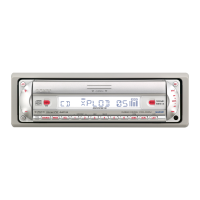
CDX-R5715X/R5810/R6750
Pin No. Pin Name I/O Pin Description
53 TU ATT IN I Tuner mute zero cross detect signal input
54 BU IN I Back-up power supply detect signal input
55 NCO O Not used
56 DAVN I RDS data block synchronized detect signal input
57 NCO O Not used
58 UNI SI I SONY bus data input
59 UNI SO O SONY bus data output
60 UNI SCK O SONY bus clock output
61 NCO O Not used
62 NCO O Not used
63 NCO O Not used
64 SIRCS I Remote control signal input
65 NCO O Not used
66 FL RST O FL driver reset output
67 NCO O Not used
68 FLASH W I Memory mode select signal input
69 NCO O Not used
70 SYNCHRO SW I Synchro CD door open/close detect signal input
71 RC IN1 I Rotary commander shift key signal input
72 ACC IN I Accessory power supply detect signal input
73 TEST IN I Test mode detect signal input
74 TEL ATT I Telephone attenuate detect signal input
75 ILLU IN I Illumination detect signal input
76 XKEY ON O A/D converter power supply control signal output
77 RESET I CPU reset input
78 NCO O Not used
79 XIN — Sub-clock input (32.768kHz)
80 XOUT — Sub-clock output (32.768kHz)
81 VSS1 — Ground
82 OSC OUT — Main-clock output (3.68MHz)
83 OSC IN — Main-clock input (3.68MHz)
84 VCC3 — Power supply pin (+3.3V)
85 DEMO SEL I Demo select signal input
86 ATT O Audio mute control signal output
87 BUS ON O Bus ON signal output
88 SYS RST O System reset output
89 EJECT OK SW O Eject OK signal output
90 NCO O Not used
91 NCO O Not used
92 NCO O Not used
93 Z-MUTE I Z-Mute signal input
94 NCO O Not used
95 NCO O Not used
96 NCO O Not used
97 NCO O Not used
98 CD ON I CD servo power control request signal input
99 CDM ON I CD deck power control request signal input
100 NCO O Not used
 Loading...