2525
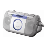
CFD-E100/E100L
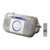
CFD-E100/E100L
• Note for Printed Wiring Boards and Schematic Diagrams
Note on Schematic Diagram:
• All capacitors are in µF unless otherwise noted. (p: pF)
50 WV or less are not indicated except for electrolytics
and tantalums.
• All resistors are in Ω and
1
/
4
W or less unless otherwise
specified.
• f : internal component.
• C : panel designation.
• A : B+ Line.
• H : adjustment for repair.
• Power voltage is dc 9V and fed with regulated dc power
supply from battery terminal.
– CD Section –
[]: CD PLAY
– TUNER Section –
no mark : FM
(): AM (MW)
< >: LW
– Other Section –
no mark : TUNER
(): CD PLAY
〈〈 〉〉 : TAPE PLAY
[]: REC
• Voltages are taken with a VOM (Input impedance 10 MΩ).
Voltage variations may be noted due to normal production
tolerances.
• Waveforms are taken with a oscilloscope.
Voltage variations may be noted due to normal production
tolerances.
• Circled numbers refer to waveforms.
• Signal path.
F : FM
f : AM (MW/LW)
J : CD PLAY
E : TAPE PLAY
a : REC
•Abbreviation
CND : Canadian model
EE : East European model
IT : Italian model
KR : Korean model
RU : Russian model
SP : Singapore model
TW : Taiwan model
Note on Printed Wiring Board:
• X : parts extracted from the component side.
• Y : parts extracted from the conductor side.
• W : indicates side identified with part number.
•
f
: internal component.
• : Pattern from the side which enables seeing.
• Circuit Boards Location
Note:
The components identi-
fied by mark 0 or dot-
ted line with mark 0 are
critical for safety.
Replace only with part
number specified.
Note:
Les composants identifiés
par une marque 0 sont cri-
tiques pour la sécurité.
Ne les remplacer que par une
piéce portant le numéro
spécifié.
TU board
BATTERY 2 board
BATTERY 1 board
MAIN board
CD board
HEADPHONE TRANSLATION board
POWER board
REMOTE CONTROL board
HEADPHONE board
LCD board
MODE board
PRE board
CD RELAY board
Ver. 1.1