20
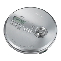
D-NE730/NE730LS/NE830/NE830LS
• IC Pin Function Description
MAIN BOARD IC801 CXR721260-201R (SYSTEM CONTROLLER)
Pin No. Pin Name I/O Description
1 TCK I JTAG Boundary Scan test clock signal input (Not used)
2 TMS I JTAG Boundary Scan testmode control signal input (Not used)
3TDI I JTAG Boundary Scan data input (Not used)
4 XTRST I JTAG Boundary Scan reset signal input (Not used)
5DVDBK — Power supply terminal (back up +1.3V)
6 XRST I System reset input terminal
7 XADEVENT O Wake signal output to power controller
8 CASINO_WAKE I Lid upper open/close detection switch input terminal
9 AN0/DCINMNT I DC in voltage detection
10 AN1/KEY1 I Key input terminal
11 AVSAD — Ground terminal
12 AN2/RMKEY I Remote control key signal input
13 AN3/BATMNT I Battery voltage detection
14 AN4/CHGMNT I Reset of rechargeable battery detection
15 AVDAD — Power supply terminal (+2.1V)
16 DVDD — Power supply terminal (+1.3V)
17 PJ0/XHOLD_I I Hold switch input terminal
18 PJ1/BOOT_SEL2 — Connected to Ground
19 PJ6/AMUTE_0 O Line out/headphone mute control signal output
20 VSS — Ground terminal
21 VDIO — Power supply terminal (+2.1V)
22 PJ7/ECO_CTL O Headphone amplifier control signal output
23 P10/LED1 O LED 1 drive control signal output
24 P12/OPSTB O Standby control signal output to pick-up
25 P13/ — Not used
26 P15/OPG UP O RF gain control signal output to pick-up
27 PI6/H-L_SEL O Headphone amplifier chip enable signal output
28 P17/VOL_LATCH — Not used
29 PE0/DBG_MNT_O/TXD I/O TX DATA signal (Not used)
30 PE1/DBG_MNT_I/RXD I/O RX DATA signal (Not used)
31 PE2/TSB O LCD indication of remote control signal output
32 PE3/XEEPROM_CS O Chip select signal output to EEPROM
33 PE4/SMUTE O Switching line/headphone signal output (L = headphone)
34 PE5/EN1/SO1 O Headphone amplifier setting control signal output
35 PE6/EN2/SI1 O Headphone amplifier setting control signal output
36 PE7/LED2 O LED 2 drive control signal output
37 PC0/XSCK0 O Clock signal output to power controller/EEPROM
38 SO0 O Serial data signal output to power controller/EEPROM
39 VSS — Ground terminal
40 SI0 I Serial data signal input from EEPROM
41 POW_LATCH O Command latch signal output to power controller
42 LINE_DTC I Line out plug insert detection signal input
43 FG I FG pulse signal input
44 TDO O Signal data output for check (Not used)
45 RTCK O Signal data output for check (Not used)
46 ATEST I Connected to Ground
47 TESTMODE I Connected to Ground