Do you have a question about the Sony DPS-V77 and is the answer not in the manual?
Procedures for measuring AC leakage current from exposed metal parts to earth ground.
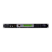
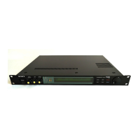
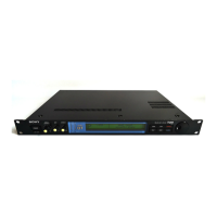
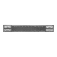
Identifies and describes the functions of the front and rear panel controls and connectors.
Explains how audio signals are processed through internal blocks and structures.
Details analog input/output handling, including priority and level adjustment.
Explains the functionality and usage of bypass and mute modes for signal routing.
Demonstrates typical connection methods for instruments and mixers.
Explains how to use digital I/O connectors for recording and digital signal input.
Step-by-step guide to select and load effects from preset and user memory.
How to activate bypass or mute functions to output original or no sound.
Configuration for seamless transitions between effects using the morphing feature.
Procedure for modifying effect parameters to create custom sounds.
Tips for faster parameter editing, such as linking channels or tap tempo.
How to alter the signal path configuration of effect blocks.
How to identify the current effect structure configuration displayed on the unit.
How to edit up to six parameters directly from the main play screen.
Procedure for designating which parameters appear for direct editing on the PLAY screen.
Assigning MIDI controllers to adjust effect parameters in real-time.
Steps to store user-created effect settings into memory banks.
How to lock user memory numbers to prevent accidental overwrites or deletions.
Procedures for copying, moving, exchanging, and deleting user memory effects.
Setting the internal clock for date and time, used for saving effects.
Adjusting noise gate attack, release, and threshold for noise reduction.
Method to mute the direct input signal, outputting only the effect sound.
Assigning functions to external pedals connected to PEDAL 1 or PEDAL 2 jacks.
References to other system settings like Bypass, Input, MIDI, User Memory, and Morphing.
Customizing the display format and contrast for readability.
Setting MIDI channel, OMNI mode, and OUT/THRU settings.
Defining how MIDI program change numbers affect memory banks and effects.
Procedure for transmitting all or selected memory data via MIDI.
Configuring which MIDI messages (exclusive, program change, control) are received.
Solutions for common operational problems like no sound or unmodifed effects.
High-level schematic showing the main functional blocks of the unit.
Steps to access the unit's self-test and diagnostic functions.
Tests for battery voltage, pedal inputs, jog/shuttle, and switches.
Checks for error messages, MIDI port, LCD, and LED functionality.
Steps to exit test mode and resume normal operation.
Identifies the clock sources for the CPU and other internal ICs.
Explains clock conditions for digital audio interface input (external vs. internal).
Detailed pin assignments and descriptions for the DSP ICs.
Pin assignments and descriptions for other integrated circuits used in the unit.
High-level schematic showing the main functional blocks of the unit.
Identifies the physical location of various circuit boards within the unit.
Detailed diagrams of the component placement on printed circuit boards.
Detailed electronic schematic of the unit's circuitry (first part).
Detailed electronic schematic of the unit's circuitry (second part).
Specific block diagrams for individual integrated circuits.
Diagram showing disassembled front panel components and their part numbers.
Diagram showing disassembled chassis components and their part numbers.
Comprehensive list of electronic components, including part numbers and descriptions.
List of screws, bolts, and other hardware used in the unit.
| A/D Conversion | 20-bit |
|---|---|
| D/A Conversion | 20-bit |
| Frequency Response | 20 Hz - 20 kHz |
| Digital Inputs | AES/EBU, S/PDIF |
| Digital Outputs | AES/EBU, S/PDIF |
| Type | Digital Effects Processor |
| Total Harmonic Distortion | < 0.05% |
| Input Connectors | XLR, 1/4" TRS |
| Output Connectors | XLR, 1/4" TRS |
| Inputs | 2 |
| Outputs | 2 |
| Effects | Reverb, Delay, Chorus, Flanger, Pitch Shift |
| THD+N | < 0.05% |
| MIDI | In, Out, Thru |
| Power Supply | 100-240V AC, 50/60Hz |