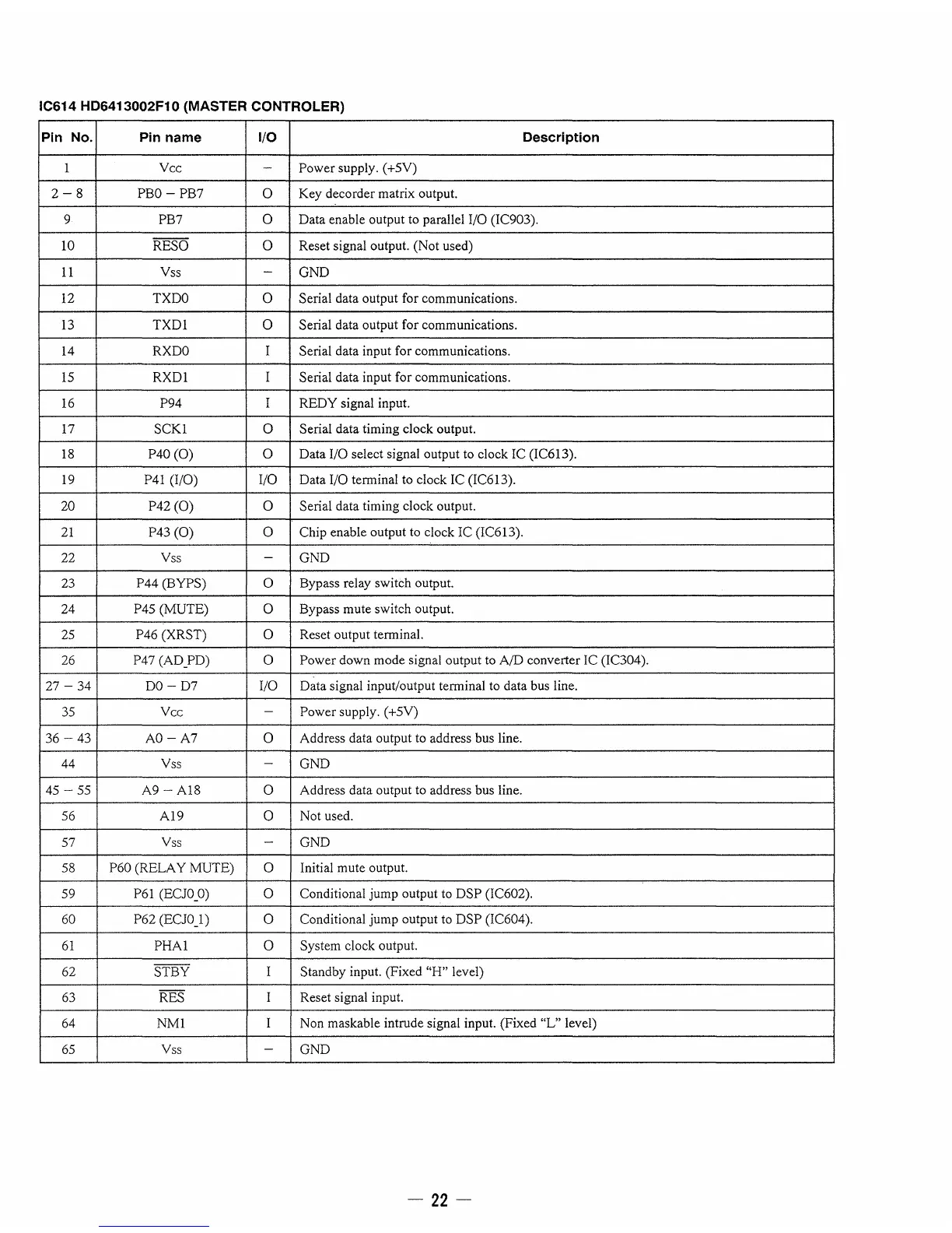
IC614 HD6413002F10 (MASTER CONTROLER)
Pin No. Pin name I/O
Description
1 Vee
-
Power supply. (+5V)
2-8
PBO
- PB7
0
Key decorder matrix output.
9
PB7 0 Data enable output to parallel I/O (IC903).
10
RESO
0
Reset signal output. (Not used)
11
Vss
-
GND
12
TXDO
0
Serial data output for communications.
13
TXDI
0
Serial data output for communications.
14
RXDO
I
Serial data input for communications.
15
RXDI
I Serial data input for communications.
16
P94 I REDY signal input.
17
SCKI 0
Serial data timing clock output.
18
P40
(0)
0
Data I/O select signal output to clock IC (IC613).
19
P41
(I/O)
I/O
Data I/O terminal to clock IC (IC613).
20 P42
(0)
0
Serial data timing clock output.
21
P43
(0)
0
Chip enable output to clock IC (IC6l3).
22
Vss
-
GND
23
P44 (BYPS) 0
Bypass relay switch output.
24
P45 (MUTE) 0
Bypass mute switch output.
25
P46 (XRST)
0
Reset output terminal.
26
P47 (AD_PD) 0
Power down mode signal output to
AID
converter IC (IC304).
27
- 34
DO-D7
I/O
Data signal input/output terminal to data bus line.
35
Vee
-
Power supply. (+5V)
36
- 43
AO-A7
0
Address data output to address bus line.
44
Vss
-
GND
45
- 55 A9 -
Al8
0
Address data output to address bus line.
56 A19
0
Not used.
57 Vss
-
GND
58
P60 (RELAY MUTE) 0
Initial mute output.
59
P6l
(EClO_O)
0
Conditional jump output to DSP (IC602).
60
P62
(EClO))
0
Conditional jump output to DSP (IC604).
61
PHAI 0
System clock output.
62
STBY
I
Standby input. (Fixed
"H" level)
63
RES
I Reset signal input.
64 NMI
I Non maskable intrude signal input. (Fixed
"L" level)
65
Vss
-
GND
-
22-