EasyManua.ls Logo

Sony HCD-GTX787 User Manual

Sony HCD-GTX787
108 pages
To Next Page IconTo Next Page
Page #1 background imageLoading...
Page #1 background image
1
HCD-GTX777/GTX787/GTX888
Ver. 1.1 2008. 05
SERVICE MANUAL
AEP Model
HCD-GTX777
E Model
HCD-GTX777/GTX787/GTX888
Australian Model
HCD-GTX888
HCD-GTX777/GTX787/GTX888
AUDIO POWER SPECIFICATION
Amplifi er section
MHC-GTX888 (HCD-GTX888)
The following are measured at
Mexican model: AC 127 V, 60 Hz
Other models: AC 120, 220, 230 – 240 V, 50/60 Hz
Front/Surround speaker
Power Output (rated): 190 W + 190 W (at 8 : and 24 :,
1 kHz, 1% THD, at LINK MODE)
RMS output power (reference):
295 W + 295 W (per channel at 8 : and
24 :, 1 kHz, 10% THD, at LINK MODE)
Subwoofer
RMS output power (reference):
160 W + 160 W (per channel at 6 :,
100 Hz, 10% THD)
SPECIFICATIONS
MHC-GTX787 (HCD-GTX787)
The following are measured at
Mexican model: AC 127 V, 60 Hz
Other models: AC 120, 220, 230 – 240 V, 50/60 Hz
Front speaker
Power Output (rated): 230 W + 230 W (at 4 :, 1 kHz, 1% THD)
RMS output power (reference):
380 W + 380 W (per channel at 4 :, 1 kHz, 10% THD)
MHC-GTX777 (HCD-GTX777)
European model only
The following are measured at
AC 230 V, 50/60 Hz
Front/Surround speaker
Power Output (rated): 235 W + 235 W (at 8 : and 8 :, 1 kHz,
1% THD, at LINK MODE)
RMS output power (reference):
380 W + 380 W (per channel at 8 : and
8 :, 1 kHz, 10% THD, at LINK MODE)
Sony Corporation
Audio Business Group
Published by Sony EMCS (Malaysia) PG Tec
9-890-504-02
2008E08-1
© 2008. 05
– Continued on next page –
CD DECK RECEIVER
• HCD-GTX777/GTX787/GTX888
are the tuner, deck, CD and
amplifi er section in
MHC-GTX777/GTX787/GTX888.
Model Name Using Similar Mechanism HCD-GTX66/GTX77/GTX88
CD
CD Mechanism Type CDM74KF-K6BD93-WOD//M
Section
Optical Pick-up Name KSM-213DCP/C2NP
Tape Deck Model Name Using Similar Mechanism NEW
Section Tape Mechanism Type CFP42608
Photo : HCD-GTX888 (E Model)

Table of Contents

Question and Answer IconNeed help?

Do you have a question about the Sony HCD-GTX787 and is the answer not in the manual?

Sony HCD-GTX787 Specifications

General IconGeneral
BrandSony
ModelHCD-GTX787
CategoryCar Receiver
TypeCD Receiver
Audio Line IN/OUTYes
Tuner BandsAM/FM

Summary

AUDIO POWER SPECIFICATIONS

Model-Specific Amplifier Details

Details amplifier section specs for GTX888, GTX787, and GTX777 models.

GENERAL SPECIFICATIONS

CD, Tape Deck, and Tuner Specs

Specifications for CD, tape deck, and tuner sections.

DETAILED SYSTEM SPECIFICATIONS

Input/Output and General System Specs

Details on inputs, outputs, power, dimensions, and mass.

Disc Player and Tape Deck Details

Specifications for disc player and tape deck sections.

Tuner, USB, and Other Model Specs

Specifications for tuner, USB, and other model variations.

REPAIR AND HANDLING GUIDELINES

Component Replacement and Repair Notes

Precautions for chip component replacement and circuit board repair.

Solder Handling and Laser Safety

Guidelines for unleaded solder and laser diode emission safety.

MODEL IDENTIFICATION

Model Number Label Information

Explains abbreviations and identifies model numbers.

SECTION 1 GENERAL

Unit Controls and Views

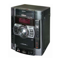
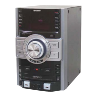
Identifies main unit parts and controls from front and top views.

REMOTE CONTROL OPERATION

Remote Control Button Functions

Descriptions of various remote control buttons and their functions.

REMOTE CONTROL DETAILS

Remote Button Usage Explanations

Continues description of remote control buttons and their operation.

REMOTE CONTROL FUNCTIONS

Function Button Operations

Explains operation of function buttons like OPTIONS, DISPLAY, CLOCK/TIMER.

SYSTEM DISPLAY INDICATORS

Display Elements and Status Lights Meaning

Explains the meaning of various display indicators and lights.

SUBWOOFER USAGE

Subwoofer A Operation Guide

Instructions on how to turn on and adjust the subwoofer level.

SECTION 2 DISASSEMBLY

Disassembly Procedure Flowchart

Provides a flowchart for the disassembly sequence.

DISASSEMBLY - CASE AND LOADING PANEL

2-1. CASE (TOP) Disassembly Steps

Steps for disassembling the top case.

2-2. LOADING PANEL Disassembly Steps

Steps for disassembling the loading panel.

DISASSEMBLY - CD AND FRONT PANEL SECTIONS

2-3. CD BLOCK SECTION Disassembly

Steps for disassembling the CD block section.

2-4. FRONT PANEL SECTION Disassembly

Steps for disassembling the front panel section.

DISASSEMBLY - TAPE MECHANISM AND BOARDS

2-5. Tape, MIC, USB Boards Disassembly

Steps for disassembling tape mechanism, MIC, USB boards.

2-6. Panel, Function, Jog Boards Disassembly

Steps for disassembling panel, function, and jog boards.

DISASSEMBLY - CD-SW AND COVER BOARDS

2-7. CD-SW BOARD Disassembly

Steps for disassembling the CD-SW board.

2-8. COVER (CDM), TC BOARD Disassembly

Steps for disassembling the CDM cover and TC board.

DISASSEMBLY - TUNER AND BACK PANEL SECTIONS

2-9. TUNER PACK Disassembly

Steps for disassembling the tuner pack.

2-10. Back Panel and Sub Trans Board Disassembly

Steps for disassembling back panel and sub trans board.

DISASSEMBLY - MAIN AND POWER BOARDS

2-11. MAIN BOARD Disassembly

Steps for disassembling the main board.

2-12. Power Board and DC Fan Disassembly

Steps for disassembling power board and DC fan.

DISASSEMBLY - SUBWOOFER AND TRANSFORMER

2-13. Subwoofer and Power Board Disassembly

Steps for disassembling subwoofer and power boards.

2-14. Power Transformer (T1200) Disassembly

Steps for disassembling the power transformer.

DISASSEMBLY - BD93 AND DRIVER BOARDS

2-15. BD93 BOARD Disassembly

Steps for disassembling the BD93 board.

2-16. Driver, SW, USB R Board Disassembly

Steps for disassembling driver, SW, and USB R boards.

DISASSEMBLY - OPTICAL PICK-UP AND SENSOR

2-17. OPTICAL PICK-UP Disassembly

Steps for disassembling the optical pick-up.

2-18. SENSOR BOARD Disassembly

Steps for disassembling the sensor board.

DISASSEMBLY - MOTOR BOARDS

2-19. MOTOR (TB) BOARD Disassembly

Steps for disassembling the motor (TB) board.

2-20. MOTOR (LD) BOARD Disassembly

Steps for disassembling the motor (LD) board.

SECTION 3 TEST MODE

GC TEST MODE Procedure

Checks fluorescent tube, LEDs, buttons, volume knob, etc.

MC TEST MODE Procedure

Checks amplifier, tuner, and tape operations.

TEST MODES - CD SECTION PROCEDURES

CD SERVICE MODE Procedure

Allows free movement of CD sled motor for cleaning.

CD AGING MODE Procedure

Performs operation check of the CD section.

TEST MODE - CD ERROR CODES

CD ERROR CODE MODE Procedure

Displays CD error codes when an error occurs.

TEST MODES - CD LIMIT AND SHIP OPTIONS

CD REPEAT 5 LIMIT OFF MODE

Enables CD playback for limitless times.

CD SHIP MODE Operation

Moves optical pick-up for vibration durability.

CD TRAY LOCK MODE Operation

Locks the disc tray to prevent opening.

SECTION 4 MECHANICAL ADJUSTMENTS

Meter Switch Touch Count Display

Displays total counts of meter pointer touch for initial and max switches.

Meter Test Mode Operation

Checks the meter device operation and step counts.

Torque Measurement Specifications

Specifies torque values for various adjustments.

SECTION 5 ELECTRICAL ADJUSTMENTS

FM Tune Level Check Procedure

Checks the FM tune level for signal reception.

CD Section Test Disc List

Lists test discs required for CD section adjustments.

S-CURVE CHECK Procedure

Checks symmetry and peak level of the S-curve waveform.

ELECTRICAL ADJUSTMENTS - CD SECTION CHECKS

S-CURVE CHECK Procedure Details

Continues checking S-curve waveform symmetry and peak levels.

RF LEVEL CHECK Procedure Details

Checks the RF signal waveform for clarity and level.

ELECTRICAL ADJUSTMENTS - RF LEVEL CHECK

RF LEVEL CHECK Procedure Details

Continues checking RF signal waveform clarity and level.

SECTION 6 DIAGRAMS

6-1. BLOCK DIAGRAM — RF/SERVO SECTION —

Block diagram of the RF and servo sections.

DIAGRAMS - TAPE/TUNER SECTIONS

6-2. BLOCK DIAGRAM — TAPE/TUNER SECTION —

Block diagram of the tape and tuner sections.

DIAGRAMS - MAIN SECTION

6-3. BLOCK DIAGRAM — MAIN SECTION —

Block diagram of the main processing section.

DIAGRAMS - USB SECTION

6-4. BLOCK DIAGRAM — USB SECTION —

Block diagram of the USB interface section.

DIAGRAMS - AMP/SUBWOOFER SECTIONS

6-5. BLOCK DIAGRAM — AMP/SUBWOOFER SECTION —

Block diagram of the amplifier and subwoofer sections.

DIAGRAMS - DISPLAY/POWER SECTIONS

6-6. BLOCK DIAGRAM — DISPLAY/POWER SECTION —

Block diagram of display and power supply sections.

CIRCUIT BOARDS LOCATIONS

6-7. CIRCUIT BOARDS LOCATION Diagram

Diagrams showing the physical location of various circuit boards.

WIRING AND SCHEMATIC DIAGRAM NOTES

Printed Wiring Board Symbols and Patterns

Explains symbols and patterns on printed wiring boards.

Schematic Diagram Conventions

Explains symbols and conventions used in schematic diagrams.

Unleaded Solder Characteristics

Details characteristics of unleaded solder.

WAVEFORM ANALYSIS

BD93 Board Waveform Examples

Displays waveforms related to CD playback on BD93 board.

Main Board Waveform Examples

Displays waveforms related to CD and USB functions on Main board.

USB Board Waveform Examples

Displays waveforms related to USB function on USB board.

PRINTED WIRING DIAGRAMS - BD93 BOARD

6-8. PRINTED WIRING BOARD — BD93 BOARD —

Printed wiring diagram for the BD93 board.

SCHEMATIC DIAGRAMS - BD93 BOARD

6-9. SCHEMATIC DIAGRAM — BD93 BOARD —

Schematic diagram for the BD93 board.

PRINTED WIRING DIAGRAMS - DRIVER BOARD AREA

6-10. PRINTED WIRING BOARDS — DRIVER BOARD —

Printed wiring diagrams for Driver, Motor, Sensor, SW boards.

SCHEMATIC DIAGRAMS - DRIVER BOARD

6-11. SCHEMATIC DIAGRAM — DRIVER BOARD —

Schematic diagram for the driver board.

PRINTED WIRING DIAGRAMS - MAIN BOARD AREA

6-12. PRINTED WIRING BOARD — MAIN BOARD —

Printed wiring diagram for the main board.

SCHEMATIC DIAGRAMS - MAIN BOARD (1/4)

6-13. SCHEMATIC DIAGRAM — MAIN BOARD (1/4) —

Schematic diagram of the main board, part 1 of 4.

SCHEMATIC DIAGRAMS - MAIN BOARD (2/4)

6-14. SCHEMATIC DIAGRAM — MAIN BOARD (2/4) —

Schematic diagram of the main board, part 2 of 4.

SCHEMATIC DIAGRAMS - MAIN BOARD (3/4)

6-15. SCHEMATIC DIAGRAM — MAIN BOARD (3/4) —

Schematic diagram of the main board, part 3 of 4.

SCHEMATIC DIAGRAMS - MAIN BOARD (4/4)

6-16. SCHEMATIC DIAGRAM — MAIN BOARD (4/4) —

Schematic diagram of the main board, part 4 of 4.

PRINTED WIRING DIAGRAMS - USB R BOARD

6-17. PRINTED WIRING BOARD — USB R BOARD —

Printed wiring diagram for the USB R board.

SCHEMATIC DIAGRAMS - USB R BOARD

6-18. SCHEMATIC DIAGRAM — USB R BOARD —

Schematic diagram for the USB R board.

PRINTED WIRING DIAGRAMS - PANEL FUNCTION BOARD

6-19. PRINTED WIRING BOARD — PANEL FUNCTION BOARD —

Printed wiring diagram for the panel function board.

SCHEMATIC DIAGRAMS - PANEL FUNCTION BOARD

6-20. SCHEMATIC DIAGRAM — PANEL FUNCTION BOARD —

Schematic diagram for the panel function board.

PRINTED WIRING DIAGRAMS - POWER BOARD

6-21. PRINTED WIRING BOARD — POWER BOARD —

Printed wiring diagram for the power board.

SCHEMATIC DIAGRAMS - POWER BOARD

6-22. SCHEMATIC DIAGRAM — POWER BOARD —

Schematic diagram for the power board.

PRINTED WIRING DIAGRAMS - SUBWOOFER BOARD

6-23. PRINTED WIRING BOARD — SUBWOOFER BOARD —

Printed wiring diagram for the subwoofer board.

SCHEMATIC DIAGRAMS - SUBWOOFER BOARD

6-24. SCHEMATIC DIAGRAM — SUBWOOFER BOARD —

Schematic diagram for the subwoofer board.

PRINTED WIRING DIAGRAMS - TRANS BOARD

6-25. PRINTED WIRING BOARDS — TRANS BOARD —

Printed wiring diagrams for the trans and sub trans boards.

SCHEMATIC DIAGRAMS - TRANS BOARD

6-26. SCHEMATIC DIAGRAM — TRANS BOARD —

Schematic diagrams for the trans and sub trans boards.

PRINTED WIRING DIAGRAMS - ILLUMINATION BOARD

6-27. PRINTED WIRING BOARDS — ILLUMINATION BOARD —

Printed wiring diagrams for illumination, USB connector, CD SW, Panel Jog boards.

SCHEMATIC DIAGRAMS - ILLUMINATION BOARD

6-28. SCHEMATIC DIAGRAM — ILLUMINATION BOARD —

Schematic diagrams for illumination, USB connector, CD SW, Panel Jog boards.

PRINTED WIRING DIAGRAMS - MIC BOARD

6-29. PRINTED WIRING BOARDS — MIC BOARD —

Printed wiring diagram for the MIC board.

SCHEMATIC DIAGRAMS - MIC BOARD

6-30. SCHEMATIC DIAGRAM — MIC BOARD —

Schematic diagram for the MIC board.

PRINTED WIRING DIAGRAMS - TC BOARD

6-31. PRINTED WIRING BOARDS — TC BOARD —

Printed wiring diagram for the TC board.

SCHEMATIC DIAGRAMS - TC BOARD

6-32. SCHEMATIC DIAGRAM — TC BOARD —

Schematic diagram for the TC board.

PRINTED WIRING DIAGRAMS - METER DISPLAY BOARD

6-33. PRINTED WIRING BOARDS — METER DISPLAY BOARD —

Printed wiring diagrams for meter display, SW, and LED boards.

SCHEMATIC DIAGRAMS - METER DISPLAY BOARD

6-34. SCHEMATIC DIAGRAM — METER DISPLAY BOARD —

Schematic diagrams for meter display, SW, and LED boards.

IC BLOCK DIAGRAMS - BD93 BOARD COMPONENTS

IC501 AK5358AET-E2 Block Diagram

Block diagram for IC501 on BD93 board.

IC401 BA5826SFP-E2 Block Diagram

Block diagram for IC401 on BD93 board.

IC BLOCK DIAGRAMS - BD93 BOARD COMPONENTS

IC502 TC74VHC157FT Block Diagram

Block diagram for IC502 on BD93 board.

IC201 TK63115SCL-G@GT Block Diagram

Block diagram for IC201 on BD93 board.

IC BLOCK DIAGRAMS - MAIN/DRIVER BOARD COMPONENTS

IC200 TC74VHC157FT Block Diagram

Block diagram for IC200 on Main board.

IC701 BA6956AN Block Diagram

Block diagram for IC701 on Driver board.

IC BLOCK DIAGRAMS - METER DISPLAY AND USB BOARDS

IC001 LB1846M (METER DISPLAY Board) Block Diagram

Block diagram for IC001 on Meter Display board.

IC915 R5523N001B-TR-F (USB Board) Block Diagram

Block diagram for IC915 on USB board.

IC BLOCK DIAGRAMS - USB AND MAIN BOARDS

IC921 IS61LV6416-10TLT (USB Board) Block Diagram

Block diagram for IC921 on USB board.

IC501 M65850FP-E1 (MAIN Board) Block Diagram

Block diagram for IC501 on Main board.

IC BLOCK DIAGRAMS - POWER AND MIC BOARDS

IC601 STK412-150C (POWER Board) Block Diagram

Block diagram for IC601 on Power board.

IC602 STK412-150C (POWER Board) Block Diagram

Block diagram for IC602 on Power board.

IC1100 NJM4558V-TE2 (MIC Board) Block Diagram

Block diagram for IC1100 on MIC board.

IC BLOCK DIAGRAMS - MAIN AND SUBWOOFER BOARDS

IC201 TC74HC4066AFT (MAIN Board) Block Diagram

Block diagram for IC201 on Main board.

IC500 TC74LVX4051FT (MAIN Board) Block Diagram

Block diagram for IC500 on Main board.

IC800 STK433-130E (SUB WOOFER Board) Block Diagram

Block diagram for IC800 on Subwoofer board.

IC BLOCK DIAGRAMS - PANEL FUNCTION AND MAIN BOARDS

IC900 BU2099FV (PANEL FUNCTION Board) Block Diagram

Block diagram for IC900 on Panel Function board.

IC902 BU2099FV (PANEL FUNCTION Board) Block Diagram

Block diagram for IC902 on Panel Function board.

IC675 S-24CS16A01-J8T1G (MAIN Board) Block Diagram

Block diagram for IC675 on Main board.

IC PIN FUNCTION DESCRIPTIONS - IC401

IC401 Pin Descriptions (1/2)

Details pin functions for IC401 (System Controller).

IC PIN FUNCTION DESCRIPTIONS - IC401 CONTINUED

IC401 Pin Descriptions (2/2)

Continues pin function details for IC401.

Other IC Pin Function Notes

General pin function notes for other ICs.

IC PIN FUNCTION DESCRIPTIONS - IC101

IC101 Pin Descriptions (1/2)

Details pin functions for IC101 (RF AMP, etc.).

IC PIN FUNCTION DESCRIPTIONS - IC101 CONTINUED

IC101 Pin Descriptions (2/2)

Continues pin function details for IC101.

IC PIN FUNCTION DESCRIPTIONS - IC901

IC901 Pin Descriptions (1/2)

Details pin functions for IC901 (USB Controller).

IC PIN FUNCTION DESCRIPTIONS - IC901 CONTINUED

IC901 Pin Descriptions (2/2)

Continues pin function details for IC901.

SECTION 7 EXPLODED VIEWS

7-1. MAIN SECTION Exploded View

Exploded view of the main section with parts list.

EXPLODED VIEWS - BACK PANEL SECTION

7-2. BACK PANEL SECTION Exploded View

Exploded view of the back panel section with parts list.

EXPLODED VIEWS - FRONT PANEL SECTION (1)

7-3. FRONT PANEL SECTION (1) Exploded View

Exploded view of the front panel, part 1.

EXPLODED VIEWS - FRONT PANEL SECTION (2)

7-4. FRONT PANEL SECTION (2) Exploded View

Exploded view of the front panel, part 2.

EXPLODED VIEWS - METER DISPLAY ASSEMBLY

7-5. METER DISPLAY ASSY Exploded View

Exploded view of the meter display assembly.

EXPLODED VIEWS - CHASSIS SECTION

7-6. CHASSIS SECTION Exploded View

Exploded view of the chassis section with parts.

EXPLODED VIEWS - CD MECHANISM SECTION (1)

7-7. CD MECHANISM SECTION (1) Exploded View

Exploded view of the CD mechanism section, part 1.

EXPLODED VIEWS - CD MECHANISM SECTION (2)

7-8. CD MECHANISM SECTION (2) Exploded View

Exploded view of the CD mechanism section, part 2.

SECTION 6 ELECTRICAL PARTS LIST

BD93 BOARD Parts List

List of electrical parts for the BD93 board.

ELECTRICAL PARTS LIST - BD93 AND CD SW BOARDS

BD93 Board Resistor and Switch List

List of resistors and switches for the BD93 board.

CD SW Board Resistor and Switch List

List of resistors and switches for the CD SW board.

ELECTRICAL PARTS LIST - DRIVER (F) AND ILLUMINATION BOARDS

Driver (F) Board Parts List

List of capacitors, connectors, diodes, ICs, transistors, and resistors for the Driver board.

Illumination Board Parts List

List of parts for the illumination board.

ELECTRICAL PARTS LIST - ILLUMINATION BOARD CONTINUED

Illumination Board Switch List

List of switches for the illumination board.

Main Board Parts List (Partial)

List of main board parts including capacitors and connectors.

ELECTRICAL PARTS LIST - MAIN BOARD

Main Board Capacitor List (Part 1)

List of capacitors for the main board.

ELECTRICAL PARTS LIST - MAIN AND TC BOARDS

Main Board Capacitor/Connector/Diode/IC List

List of capacitors, connectors, diodes, and ICs for the main board.

TC BOARD Parts List

List of capacitors, connectors, diodes, ICs, transistors, and resistors for the TC board.

ELECTRICAL PARTS LIST - TC AND TRANSISTOR COMPONENTS

TC Board Transistor and Resistor List

List of transistors and resistors for the TC board.

ELECTRICAL PARTS LIST - RESISTORS

Resistor List (Main Board Part 1)

List of resistors for the main board.

ELECTRICAL PARTS LIST - RESISTORS CONTINUED

Resistor List (Main Board Part 2)

List of resistors for the main board.

ELECTRICAL PARTS LIST - RESISTORS AND METERS

Resistor List (Main Board Part 3)

List of resistors for the main board.

METER DISPLAY BOARD Parts List

List of parts for the meter display board.

ELECTRICAL PARTS LIST - METER DISPLAY AND MIC BOARDS

METER DISPLAY SW BOARD Parts List

List of parts for the meter display SW board.

MIC BOARD Parts List

List of capacitors, diodes, ICs, jacks, and resistors for the MIC board.

ELECTRICAL PARTS LIST - SWITCHES AND RESISTORS

Panel Function Board Switch List

List of switches for the panel function board.

Resistor List (Panel Function Board)

List of resistors for the panel function board.

ELECTRICAL PARTS LIST - PANEL JOG AND POWER BOARDS

Panel Jog Board Parts List

List of capacitors, resistors, switches, and encoders for the panel jog board.

Power Board Parts List

List of parts for the power board.

ELECTRICAL PARTS LIST - POWER AND SUB TRANS BOARDS

Power Board Resistor and Transistor List

List of resistors and transistors for the power board.

Sub Trans Board Parts List

List of capacitors, connectors, diodes, and transistors for the sub trans board.

ELECTRICAL PARTS LIST - SUB WOOFER BOARD

Sub Woofer Board Parts List

List of capacitors, connectors, diodes, ICs, transistors, and resistors for the sub woofer board.

ELECTRICAL PARTS LIST - SW, TC, AND TRANSISTOR COMPONENTS

SW Board Parts List

List of capacitors, connectors, diodes, ICs, transistors, and resistors for the SW board.

TC Board Parts List

List of capacitors, connectors, diodes, ICs, transistors, and resistors for the TC board.

ELECTRICAL PARTS LIST - TRANS AND USB R BOARDS

Trans Board Parts List

List of capacitors, connectors, diodes, fuses, and transistors for the trans board.

USB R Board Parts List

List of capacitors, connectors, diodes, and jumpers for the USB R board.

ELECTRICAL PARTS LIST - USB CONNECTOR BOARD

USB Connector Board Parts List

List of parts for the USB connector board.

MISCELLANEOUS COMPONENTS

Miscellaneous Parts List

List of miscellaneous parts including wires, adaptors, cords, magnet assy, fuses, and fans.

Related product manuals