EasyManua.ls Logo

Sony HCD-SLK1i - Dvd Receiver User Manual

Sony HCD-SLK1i - Dvd Receiver
88 pages
To Next Page IconTo Next Page
Page #1 background imageLoading...
Page #1 background image
SERVICE MANUAL
Sony Corporation
Audio&Video Business Group
Published by Sony Techno Create Corporation
USB section
(USB) port: Type A
Maximum current: 500 mA
Memory card section
Multi memory card slot:
Compatible with “Memory Stick”
media (page 110), SD memory cards
(page 111)
Disc player section
System:
Compact disc and digital audio and
video system
Laser Diode Properties
Emission duration: Continuous
Laser Output*: Less than 44.6 µW
* is output is the value measurement
at a distance of 200mm from the
objective lens surface on the Optical
Pick-up Block with 7mm aperture.
Frequency response
DVD (PCM 48 kHz): 2 Hz
22 kHz
(±1 dB)
CD: 2 Hz
20 kHz (±0.5 dB)
Video color system format
North American and Latin American
models: NTSC
Other models: NTSC and PAL
Tuner section
FM stereo, FM/AM superheterodyne tuner
FM tuner section
Tuning range
North American and Brazilian
models:
87.5 MHz
108.0 MHz (100 kHz
step)
Other models:
87.5 MHz
108.0 MHz (50 kHz step)
Main unit
AUDIO POWER SPECIFICATIONS
POWER OUTPUT AND TOTAL
HARMONIC DISTORTION:
(HCD-SLK1i e United States model
only)
With 8 ohm loads, both channels driven,
from 120
10,000 Hz; rated 35 watts per
channel minimum RMS power, with no
more than 1% total harmonic distortion
from 800 milliwatts to rated output.
Amplier section
e following measured at AC 120 V, 60 Hz
(North American model)
e following measured at AC 127 V, 60 Hz
(Mexican model)
e following measured at AC 127 V
240 V, 60 Hz (Brazilian model)
e following measured at AC 220 V
240 V, 50/60 Hz (European, Korean,
Argentine and ai models)
e following measured at AC 120 V
240 V, 50/60 Hz (Other models)
HCD-SLK2i
Brazilian model:
Power output (rated):
85 W + 85 W (at 6 , 1 kHz,
1% THD)
RMS output power (reference):
100 W + 100 W (per channel at 6 ,
1 kHz, 10% THD)
Other models:
Power output (rated):
85 W + 85 W (at 6 , 1 kHz,
1% THD)
RMS output power (reference):
120 W + 120 W (per channel at 6 ,
1 kHz)
HCD-SLK1i
e United States model:
RMS output power (reference):
65 W + 65 W (per channel at 8 ,
1 kHz)
Other models:
Power output (rated):
40 W + 40 W (at 8 , 1 kHz,
1% THD)
RMS output power (reference):
65 W + 65 W (per channel at 8 ,
1 kHz)
General
Power requirements
North American model:
AC 120 V, 60 Hz
Mexican model:
AC 127 V, 60 Hz
Brazilian model:
AC 127 V
240 V, 60 Hz
European, Korean, Argentine and
ai models:
AC 220 V
240 V, 50/60 Hz
Other models:
AC 120 V
240 V, 50/60 Hz
Power consumption
HCD-SLK2i:
80 W
HCD-SLK1i:
60 W
Dimensions (W/H/D) (excl. speakers)
HCD-SLK2i:
Approx. 330 mm × 203 mm ×
141 mm
HCD-SLK1i:
Approx. 330 mm × 203 mm ×
138 mm
Mass (excl. speakers)
HCD-SLK2i:
Approx. 3.7 kg
HCD-SLK1i:
Approx. 3.6 kg
iPod models
You can use the following iPod models on this system. Update your iPod with the latest
soware before using it.
iPod nano
5th generation
(video camera)
iPod touch
2nd generation
iPod classic
120 GB
160 GB (2009)
iPod nano
4th generation
(video)
iPod classic
160 GB (2007)
iPod touch
1st generation
iPod nano
3rd generation
(video)
iPod classic
80 GB
iPod nano
2nd generation
(aluminum)
Design and specications are subject to
change without notice.
Outputs
DVD VIDEO OUT:
max. output level 1 Vp-p, unbalanced,
Sync negative, load impedance 75 
PHONES:
accepts headphones of 8  or more
SPEAKERS:
Use only the supplied speakers
SS-SLK2i (WHG-SLK2i) or SS-SLK1i
(WHG-SLK1i).
AM tuner section
Tuning range
European and Saudi Arabian models:
531 kHz
1,602 kHz (9 kHz step)
North American and Latin American
models:
530 kHz
1,710 kHz (10 kHz step)
531 kHz
1,710 kHz (9 kHz step)
Other models:
531 kHz
1,602 kHz (9 kHz step)
530 kHz
1,610 kHz (10 kHz step)
Antenna:
AM loop antenna
Antenna terminals:
External antenna terminal
Intermediate frequency:
450 kHz
Inputs
VIDEO/SAT VIDEO IN:
1 Vp-p, 75 
VIDEO/SAT AUDIO IN:
voltage 250/450 mV, impedance
47 k
Antenna:
FM lead antenna
Antenna terminals:
75 Ω unbalanced
Intermediate frequency:
10.7 MHz
HCD-SLK1i/SLK2i
SPECIFICATIONS
DVD RECEIVER
9-889-894-01
2010F05-1
©
2010.06
US Model
Canadian Model
AEP Model
Chinese Model
Saudi Arabia Model
Singapore Model
Korean Model
Thai Model
HCD-SLK1i
Mexican Model
Brazilian model
Argentina model
HCD-SLK2i
E Model
HCD-SLK1i/SLK2i
Ver. 1.0 2010.06
Model Name Using Similar Mechanism NEW
Mechanism Type CDM86B-DVBU101
Optical Pick-up Name KHM-313CAB
HCD-SLK1i is the ampli er, USB, memory card, disc player and tuner section in WHG-SLK1i.
HCD-SLK2i is the ampli er, USB, memory card, disc player and tuner section in WHG-SLK2i.
Photo: HCD-SLK1i

Table of Contents

Question and Answer IconNeed help?

Do you have a question about the Sony HCD-SLK1i - Dvd Receiver and is the answer not in the manual?

Sony HCD-SLK1i - Dvd Receiver Specifications

General IconGeneral
BrandSony
ModelHCD-SLK1i - Dvd Receiver
CategoryReceiver
LanguageEnglish

Summary

Product Specifications

Audio Power Specifications

Details audio output power and distortion based on load and voltage.

Input/Output Terminals

Lists video, audio, speaker, and headphone connection specifications.

Disc Player Specifications

Covers laser diode properties, frequency response, and video color systems.

Tuner Specifications

Details FM/AM tuning ranges, antenna types, and intermediate frequencies.

General Specifications

Includes power requirements, consumption, dimensions, and mass.

Supported iPod Models

Lists compatible iPod models for use with the system.

Safety Precautions and Checks

Safety Check-out Procedure

Steps to perform after service to ensure customer safety.

AC Leakage Test

Method for measuring AC leakage current from exposed metal parts.

Component Replacement Safety

Warning about critical components and replacement procedures.

Servicing and Handling Notes

Optical Pick-up Handling

Precautions for handling the optical pick-up block to prevent damage.

Laser Diode Emission Check

Guidance on how to safely check laser diode emission.

Unleaded Solder Usage

Characteristics and handling of unleaded solder for repairs.

Disc Slot Lock Release

Procedure to unlock the disc slot for sample discs.

Main Board Identification

Distinguishing between SUFFIX-11 and SUFFIX-12 main boards.

Capacitor Discharge Procedure

Capacitor Electrical Discharge Processing

Steps to safely discharge capacitors before board inspection.

Service Positions and Ejection Procedures

Ejecting Disc Without Power

Method to eject a disc when the system power is off.

IP Board Service Position

Illustration showing the service position for the IP board.

Board Service Connections

Main Board Service Position

Instructions for connecting extension jigs to the main board.

Switching Regulator Service Position

Instructions for connecting extension jigs to the switching regulator.

Component Board Service Positions

Display Board Service Position

Guidelines for connecting extension jigs to the display board.

DVD, LCD, and Jack Board Service Positions

Instructions for connecting extension jigs to DVD, LCD, and Jack boards.

Disassembly Procedure Overview

Disassembly Flow

Visual flow chart detailing the order of set disassembly.

External Component Disassembly

Top Panel Block Removal

Step-by-step guide for removing the top panel.

Rear Case Block Removal

Instructions for disassembling the rear case.

Chassis and Internal Component Disassembly

Main Chassis Block Disassembly

Procedure for accessing the main chassis block and its components.

Internal Board Disassembly

Main Board Removal

Steps to remove the main board from the unit.

Switching Regulator Block Removal

Procedure for disassembling the switching regulator block.

Mechanism and Cover Disassembly

Cover (CDM) Block Removal

Instructions for removing the CDM cover block.

DVD Mechanism Deck Block Removal

Steps for disassembling the DVD mechanism deck block.

Display Module Disassembly

Display Board Removal

Procedure for removing the display board assembly.

Core Component Disassembly

Optical Pick-up Block Removal

Steps to remove the KHM-313CAB optical pick-up block.

Belt (MOT) Replacement

Procedure for accessing and replacing the motor belt.

Display Panel Disassembly

LCD Board Removal

Instructions for removing the LCD board.

LCD Module Disassembly

Steps for disassembling the LCD module itself.

System Test Modes

Cold Reset Procedure

Resets the system to factory default settings.

Common Test Mode

Executes all tests in each category.

Version Display Mode

Shows system, GUI, DVD, destination, and model names.

VACS Display Mode

Displays VACS levels based on blinking frequency.

DVD Ship Mode and Cold Reset

Resets system and enters DVD ship mode simultaneously.

Video/Sat Source Change

Allows changing the external video source between Video and Satellite.

Special Operation Modes

Disc Antitheft Lock

Mode to prevent sample disc removal from the slot.

DVD Color System Change

Changes video output color system between PAL and NTSC.

MTK Reboot Prevent Setting

Sets MTK to prevent rebooting.

Tuner Step Change

Toggles AM channel step between 9 kHz and 10 kHz.

Remote Disable Mode

Disables remote commander reception.

DVD Service Mode Entry

How to enter DVD service mode using the remote commander.

Diagnostic Procedures

Executing IOP Measurement

Standard procedures for IOP measurement and diagnosis.

Emergency History Check

How to check the emergency history log for errors.

Diagnosis Menu Operations

Clearing Laser Hours and History

Procedures to clear laser hours, emergency history, and setup data.

Checking Version Information

How to view system version information from the diagnosis menu.

Block Diagrams

Servo Section Block Diagram

Diagram showing the signal flow and components of the servo section.

Block Diagrams

Audio Input Section Block Diagram

Diagram illustrating the audio input signal paths and related components.

Block Diagrams

Audio Output Section Block Diagram

Diagram showing the audio output signal paths, including digital power amp.

Block Diagrams

Video Section Block Diagram

Diagram illustrating video input, processing, and output paths.

Block Diagrams

Panel and Power Supply Section Block Diagram

Diagram showing power supply circuits and panel control.

Document Notes and Board Locations

Printed Wiring Board Notes

Guidelines for interpreting printed wiring board diagrams.

Schematic Diagram Notes

Notes on interpreting schematic diagrams and component markings.

Circuit Board Location Overview

Visual map showing the physical locations of various circuit boards.

Display Board Schematics

Display Section Schematic (1/7)

First part of the schematic diagram for the display board.

Display Board Schematics

Display Section Schematic (2/7)

Second part of the schematic diagram for the display board.

Display Board Schematics

Display Section Schematic (3/7)

Third part of the schematic diagram for the display board.

Display Board Schematics

Display Section Schematic (4/7)

Fourth part of the schematic diagram for the display board.

Display Board Schematics

Display Section Schematic (5/7)

Fifth part of the schematic diagram for the display board.

Display Board Schematics

Display Section Schematic (6/7)

Sixth part of the schematic diagram for the display board.

Display Board Schematics

Display Section Schematic (7/7)

Seventh and final part of the schematic diagram for the display board.

Printed Wiring Boards

Display Section PWB (1/2)

First part of the printed wiring board layout for the display section.

Printed Wiring Boards (Continued)

Display Section PWB (2/2)

Second part of the printed wiring board layout for the display section.

LCD Board Printed Wiring

LCD Board PWB Layout

Printed wiring board layout for the LCD board, showing component placement.

LCD Board Schematic

LCD Board Schematic Diagram

Schematic diagram detailing the circuitry of the LCD board.

Audio Section Printed Wiring

Audio IN/OUT Section PWBs

Printed wiring board layouts for HP, Terminal, Jack, and IP boards.

Audio Section Schematics

Audio IN/OUT Section Schematics

Schematic diagrams for HP, Terminal, Jack, and IP boards.

Key Section Printed Wiring

Key Section PWBs

Printed wiring board layouts for the key left and key right boards.

Key Section Schematic

Key Section Schematic Diagram

Schematic diagram detailing the circuitry of the key left and key right boards.

Main Board Printed Wiring (SUFFIX-11)

Main Board Component Side (SUFFIX-11)

Printed wiring board layout of the main board's component side for SUFFIX-11.

Main Board Printed Wiring (SUFFIX-11) (Continued)

Main Board Conductor Side (SUFFIX-11)

Printed wiring board layout of the main board's conductor side for SUFFIX-11.

Main Board Printed Wiring (SUFFIX-12)

Main Board Component Side (SUFFIX-12)

Printed wiring board layout of the main board's component side for SUFFIX-12.

Main Board Printed Wiring (SUFFIX-12) (Continued)

Main Board Conductor Side (SUFFIX-12)

Printed wiring board layout of the main board's conductor side for SUFFIX-12.

Main Board Schematics

Main Board Schematic (1/4)

First part of the schematic diagram for the main board.

Main Board Schematics

Main Board Schematic (2/4)

Second part of the schematic diagram for the main board.

Main Board Schematics

Main Board Schematic (3/4)

Third part of the schematic diagram for the main board.

Main Board Schematics

Main Board Schematic (4/4)

Fourth part of the schematic diagram for the main board.

Waveforms and IC Block Diagrams

Waveforms

Oscilloscope waveforms for key test points on display and main boards.

IC Block Diagrams

Block diagrams illustrating the internal functions of key ICs.

Integrated Circuit Block Diagrams

IC602, IC603/604, IC605 Block Diagrams

Block diagrams detailing the internal structure of specific integrated circuits.

Integrated Circuit Block Diagrams

IC606, IC610, IC1001 Block Diagrams

Block diagrams for IC606, IC610, and IC1001 showing internal logic.

Integrated Circuit Block Diagrams

IC500 Block Diagram

Block diagram illustrating the internal functions of IC500.

Integrated Circuit Block Diagrams

IC900, IC901, IC907, IC908 Block Diagrams

Block diagrams for IC900, IC901, IC907, and IC908 showing internal functions.

IC Pin Function Descriptions

Display Board IC005 Pin Functions

Detailed pinout description for IC005 on the display board.

IC Pin Function Descriptions

Display Board IC005 Pin Functions (Continued)

Continuation of pinout descriptions for IC005 on the display board.

IC Pin Function Descriptions

Display Board IC401 Pin Functions

Detailed pinout description for IC401 on the display board.

IC Pin Function Descriptions

Display Board IC401 Pin Functions (Continued)

Continuation of pinout descriptions for IC401 on the display board.

IC Pin Function Descriptions

Display Board IC401 Pin Functions (Continued)

Continuation of pinout descriptions for IC401 on the display board.

IC Pin Function Descriptions

Main Board IC100 Pin Functions

Detailed pinout description for IC100 on the main board.

IC Pin Function Descriptions

Main Board IC100 Pin Functions (Continued)

Continuation of pinout descriptions for IC100 on the main board.

IC Pin Function Descriptions

Main Board IC300 Pin Functions

Detailed pinout description for IC300 on the main board.

IC Pin Function Descriptions

Main Board IC300 Pin Functions (Continued)

Continuation of pinout descriptions for IC300 on the main board.

Exploded Views

Top Panel and Rear Case Assembly

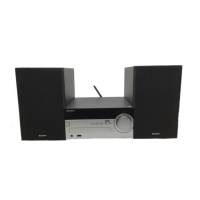
Exploded view showing the parts for the top panel and rear case assembly.

Switching Regulator Section Exploded View

Switching Regulator Components

Exploded view illustrating the components of the switching regulator section.

Main Board Section Exploded View

Main Board Assembly Exploded View

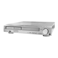
Exploded view showing the main board and related components.

Display Board Section Exploded View

Display Board Assembly Exploded View

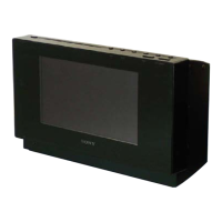
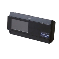
Exploded view illustrating the parts of the display board assembly.

Front Panel Section Exploded View

Front Panel Assembly Exploded View

Exploded view showing the components of the front panel assembly.

DVD Mechanism Deck Exploded View

DVD Mechanism Deck Assembly (CDM86B-DVBU101)

Exploded view of the DVD mechanism deck section, including the optical pick-up block.

Electrical Parts List

Display Board Parts List

Comprehensive list of electrical components for the display board.

Electrical Parts List (Continued)

Display Board Parts List (Continued)

Continuation of the electrical components list for the display board.

Electrical Parts List (Continued)

Display Board Parts List (Continued)

Further continuation of the electrical components list for the display board.

Electrical Parts List (Continued)

Connectors, Diodes, Ferrites, Filters, and ICs

List of connectors, diodes, ferrite beads, filters, and integrated circuits.

Electrical Parts List (Continued)

ICs, Vibrators, Terminals, Diodes, Transistors, and Resistors

List of ICs, vibrators, terminals, diodes, transistors, and resistors.

Electrical Parts List (Continued)

Resistor List (Continued)

Continuation of the resistor list with various part numbers and values.

Electrical Parts List (Continued)

Resistor List (Continued)

Further continuation of the resistor list with various part numbers and values.

Electrical Parts List (Continued)

Resistor List (Continued)

Final part of the resistor list with various part numbers and values.

Electrical Parts List (Continued)

Connectors, Diodes, ICs, Buzzers, and Capacitors

List of connectors, diodes, ICs, buzzers, and capacitors for various boards.

Electrical Parts List (Continued)

Jacks, Resistors, Switches, and LCD Capacitors

List of jacks, resistors, switches, and capacitors for LCD board.

Electrical Parts List (Continued)

LCD/Main Board Components

List of connectors, LEDs, transistors, resistors, and capacitors for LCD and Main boards.

Electrical Parts List (Continued)

Main Board Capacitors

List of capacitors used on the main board.

Electrical Parts List (Continued)

Main Board Capacitors, Connectors, and Diodes

List of capacitors, connectors, and diodes for the main board.

Electrical Parts List (Continued)

Diodes, Ferrites, Filters, ICs, Resistors, and Transistors

List of diodes, ferrite beads, filters, ICs, jumper resistors, coils, photo diode, and transistors.

Electrical Parts List (Continued)

Resistor List (Continued)

Continuation of the resistor list with various part numbers and values.

Electrical Parts List (Continued)

Resistor List (Continued)

Further continuation of the resistor list with various part numbers and values.

Electrical Parts List (Continued)

Resistors, Terminals, Connectors, and Touch Panel Components

List of resistors, terminals, connectors, and touch panel components.

Electrical Parts List (Continued)

Miscellaneous Parts List

List of miscellaneous parts including cores, cords, filters, wires, and assemblies.

Revision History

Revision History Record

Records of revisions made to the service manual.

Related product manuals