Do you have a question about the Sony KE-P42M1 and is the answer not in the manual?
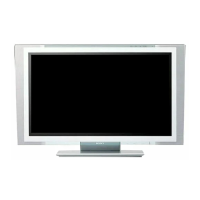
Details of the television's display panel specifications.
Specifies the necessary AC voltage and frequency for operation.
Indicates the diagonal measurement of the display screen.
Lists the number of pixels horizontally and vertically.
States the typical power draw during operation.
Details the power used when the unit is in standby mode.
Provides the physical size of the unit with and without stand.
Lists the weight of the unit with and without stand.
Identifies the type of display panel used.
Lists supported broadcast TV system standards.
Specifies supported color standards for TV signals.
Describes the type of antenna input terminal.
Details the range of TV channels supported by frequency bands.
Describes the various input/output connectors on the unit.
Specifies the audio output power.
Lists items included in the product package.
Lists accessories available for separate purchase.
Highlights additional functionalities of the television.
Procedure to measure and verify AC leakage current from metal parts.
Instructions for detaching the rear cover and stand.
Steps to remove the main internal metal shield.
Procedure for removing the J and UPE circuit boards.
Steps to remove the AE and BP circuit boards.
Instructions for removing the F and G2 circuit boards.
Steps to remove the G1 circuit board.
Procedure for safely removing the Plasma Display Panel.
Steps to remove the H1 and H3 circuit boards.
Instructions for removing the H2 circuit board.
Procedures for setting and performing the aging process for the unit.
Steps for calibrating signal levels using the ECS.
Verifying calibration items for 2163 case signal input.
Calibrating Y signal levels for 2163 decode.
Calibrating C signal levels for 2163 decode.
Verifying calibration items for CCP2 case signal input.
Calibrating Y signal levels for CCP2 decode.
Calibrating C signal levels for CCP2 decode.
Verifying calibration items for component signal input.
Calibrating Y signal levels for component input.
Calibrating C signal levels for component input.
Procedure for adjusting white balance for different color temperatures.
High-level functional block diagram of the system.
Illustrates the physical layout of major internal components.
Shows the physical placement of circuit boards within the unit.
Detailed circuit schematics and PCB layout diagrams for various boards.
Identification and diagrams of semiconductor components used.
Exploded view showing the rear cover and stand assembly.
Exploded view detailing parts of the main chassis assembly.
Exploded view showing additional parts of the main chassis assembly.
Exploded view of the front bezel and associated parts.
Lists components and materials used for product packaging.
List of capacitors used on the UPE board.
List of capacitors used on the BP board.
List of capacitors used on the AE board.
List of capacitors used on the G1 board.
List of capacitors used on the G2 board.
| Depth | 110 mm |
|---|---|
| Width | 1075 mm |
| Height | 750 mm |
| Weight | 39500 g |
| I/O ports | 4 Pin (Y/C) In RCA Audio Out RCA AV Input RF In Scart 1 (RGB) Scart 2 (RGB) Scart 3 (Smartlink) Component |
| Product color | Silver |
| Display diagonal | 42 \ |
| Sound output mode | Virtual Dolby Surround Sound |
| Display resolution | 852 x 480 pixels |
| Display technology | Plasma |
| Contrast ratio (typical) | 550:1 |
| Power consumption (typical) | 365 W |