Do you have a question about the Sony KLV-V26A10E and is the answer not in the manual?
Precautions for servicing boards using lead-free solder material and recommended parts.
Details on power, dimensions, weight, and general operational characteristics.
Description of rear and side connection panels and their pin configurations.
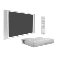
List of accessories included with the product for operation and installation.
Instructions and warnings regarding fuse replacement for UK models.
Table indicating the operational status (ON/OFF) of various model features.
Detailed pinout and signal level specifications for the 21-pin SCART connector.
Pinout and signal level specifications for the S-Video socket.
Explanation of how the AT2X chassis identifies errors via busy states or device failures.
Table detailing LED error codes and their corresponding error descriptions.
Step-by-step guide for connecting external video sources like aerials and VCRs.
Procedure for tuning the TV to receive available digital and analogue channels.
How to access and use the EPG to view program information and set recordings.
Instructions for displaying video from external devices connected via SCART or other inputs.
Guide on navigating through the TV's menu system using the remote control.
Adjusting picture modes, color tone, contrast, brightness, and other visual settings.
Configuring sound effects, treble, bass, balance, and auto volume settings.
Adjusting screen format, auto format, and picture position for optimal display.
Configuring power saving, internal speakers, and AV output settings.
Setting sleep timer and auto shutoff for power management and convenience.
Configuring initial setup, auto tuning, programme sorting, and AV presets.
Guide on connecting various external devices like camcorders and headphones.
Assigning names to channels and configuring AV input presets for connected devices.
Instructions for manually setting up and skipping input sources or programmes.
Diagram illustrating the layout and connections available on the rear panel.
Comprehensive list of specifications including power, dimensions, mass, and system details.
Diagnosing issues based on the flashing pattern of the standby indicator.
Common causes and remedies for picture, sound, and channel reception problems.
Resolving issues related to automatic power-off, input selection, remote control, and indicator flashes.
Step-by-step instructions for removing the rear cover of the TV set.
Instructions for safely removing internal brackets from the TV chassis.
Procedure for removing the left and right loudspeakers from the TV.
Instructions for removing the A1 (26-inch) or A2 (32-inch) main circuit boards.
Step-by-step guide for removing the G2 circuit board.
Instructions for removing the H7 circuit board.
Procedure for removing the H8 circuit board.
Instructions for removing the BL, N, and NP1 circuit boards.
Step-by-step instructions for removing the H6 circuit board.
Steps to place the TV in a service position for internal component access and testing.
Instructions on reconnecting circuit boards and using specific service cables.
Details on using the IF board to mount the A1 board vertically for service access.
Procedure for entering and navigating the service menu using the remote commander.
Calibration steps for Y and C signals in CCPX decode mode.
Calibration procedures for Y and C signals using component video input.
Procedure for adjusting white balance for the 'Cool' color temperature setting.
Procedure for adjusting white balance for the 'Neutral' color temperature setting.
Procedure for adjusting white balance for the 'Warm' color temperature setting.
Note on readjusting white balance after panel replacement.
Guidance on adjustments required after replacing P, BL, A1, or A2 boards.
Checking AD calibration registration items using AV1 and PAL signal.
Detailed steps for Y signal AD calibration in CCPX decode using ECS.
Detailed steps for C signal AD calibration in CCPX decode using ECS.
Checking AD calibration registration items for component input signals.
Detailed steps for Y signal AD calibration of component input.
Detailed steps for C signal AD calibration of component input.
Step-by-step guide for adjusting white balance for 'Cool' color temperature.
Step-by-step guide for adjusting white balance for 'Neutral' color temperature.
Step-by-step guide for adjusting white balance for 'Warm' color temperature.
Block diagram illustrating the main functional areas and interconnections on the A1 board.
Further illustration of A1 board block diagram showing module connections.
Block diagram showing the main functional units and signal paths on the A2 board.
Further illustration of A2 board block diagram detailing module interconnections.
Block diagram illustrating the power supply functions of the G2 board.
Block diagram showing the D-D converters on the NP1 board.
Block diagram detailing the digital decoding functions of the N board.
Diagram showing the physical location of major circuit boards within the TV.
Important notes and symbols used in schematic diagrams and printed wiring boards.
Schematic details of the voltage regulator circuits on the A1 board.
Schematic details of the audio processor, headphone, and audio output circuits.
Schematic diagram of the main processor and its associated components on the A1 board.
Schematic details of the tuner block and related components on the A1 board.
Schematic of A1 board showing Y/C inputs and SCART connector circuits.
Schematic of circuits handling audio and video switching on the A1 board.
Schematic details of the video processing circuits on the A1 board.
Diagram showing the component layout on the conductor side A of the A1 board.
Table listing semiconductor locations on the A1 board, side A.
Table detailing differences in components between KDL and KLV models for A1 board.
Diagram showing the component layout on the conductor side B of the A1 board.
Table listing semiconductor locations on the A1 board, side B.
Schematic details of the voltage regulator circuits on the A2 board.
Schematic details of the audio processor, headphone, and audio output circuits.
Schematic diagram of the main processor and its associated components on the A2 board.
Schematic details of the tuner block and related components on the A2 board.
Schematic of A2 board showing Y/C inputs and SCART connector circuits.
Schematic of circuits handling audio and video switching on the A2 board.
Schematic details of the video processing circuits on the A2 board.
Diagram showing component layout on the conductor side A of the A2 board.
Table listing semiconductor locations on the A2 board, side A.
Table of measured voltages for IC components on the A2 board, side A.
Table detailing component differences between KDL and KLV models for A2 board.
Table of measured voltages for IC components on the A2 board.
Diagram showing component layout on the conductor side B of the A2 board.
Table listing semiconductor locations on the A2 board, side B.
Schematic details of the power supply circuits on the G2 board.
Diagram showing component layout on the conductor side A of the G2 board.
Table listing semiconductor locations on the G2 board, side A.
Diagram showing component layout on the conductor side B of the G2 board.
Table listing semiconductor locations on the G2 board, side B.
Schematic details of the digital decoder section on the N board.
Schematic details of NAND flash memory interface and CPU clock generation.
Schematic details of buffer circuits and PCMCIA interface on the N board.
Schematic details of video circuit, audio DAC, and power switches on the N board.
Schematic details of analog IF, GSI/Modem power, and SPDIF output circuits.
Schematic details of the smartcard and modem interface circuits on the N board.
Schematic details of the tuner and FSS circuitry on the N board.
Schematic details of JTAG connections and other interface circuits on the N board.
Schematic details of the reset signal generation circuit on the N board.
Schematic details of the EEPROM and option select resistor configurations.
Diagrams showing component layout on both sides of the N board's PWB.
Tables listing semiconductor locations on both sides of the N board.
Table of measured voltages for IC components on the N board.
Schematic diagram of the key switch circuit on the H6 board.
Schematic diagram of the LED and Sircs (infrared receiver) circuits on the H7 board.
Schematic diagram of the AV input/output circuits on the H8 board.
Printed wiring board layout for the H6 board.
Printed wiring board layout for the H7 board.
Printed wiring board layout for the H8 board.
Schematic details of the D-D converter circuits on the NP1 board.
Diagrams showing component layout on both sides of the NP1 board's PWB.
Tables listing semiconductor locations for the NP1 board, sides A and B.
Table detailing component differences between KDL and KLV models for NP1 board.
Visual reference and names for various semiconductor components used in the manual.
Exploded view illustrating the main chassis components and their assembly.
List of part numbers and descriptions for chassis construction components.
Exploded view illustrating the display unit and its assembled parts.
List of part numbers and descriptions for display assembly components.
List of additional display assembly components including covers, boards, and AC inlet.
List of part numbers and specifications for capacitors used on the NP1 board.
List of part numbers for connectors, diodes, and ferrite beads on the NP1 board.
List of part numbers and types for ICs and filters on the NP1 board.
List of part numbers and specifications for resistors on the NP1 board.
List of part numbers for transistors, coils, and connectors on the NP1 board.
List of part numbers for ferrite beads on the NP1 board.
List of part numbers and types for ICs and diodes on the NP1 board.
List of part numbers and types for IC components on the G2 board.
List of part numbers for coils, transistors, and resistors on the G2 board.
List of part numbers and specifications for resistors on the G2 board.
List of part numbers for connectors, diodes, and ferrite beads on the G2 board.
List of part numbers for ICs, coils, transistors, varistors, and crystals on the G2 board.
List of part numbers and specifications for resistors on the G2 board.
List of part numbers and specifications for resistors on the G2 board.
List of part numbers for ICs, connectors, diodes, and ferrite beads on the G2 board.
List of part numbers for diodes on the G2 board.
List of part numbers for ferrite beads, ICs, coils, and fuses on the G2 board.
List of part numbers for connectors, transistors, varistors, and crystals on the G2 board.
List of part numbers for coils on the G2 board.
List of part numbers for transistors on the G2 board.
List of part numbers for resistors on the G2 board.
List of part numbers for resistors on the G2 board.
List of part numbers for connectors, diodes, ferrite beads, and ICs on the G2 board.
Parts lists for the H6, H7, and H8 circuit boards.
List of part numbers for diodes and ICs on the A1 board for KLV-V26A10E.
List of part numbers for transistors and resistors on the A1 board for KLV-V26A10E.
List of part numbers for connectors and capacitors on the A1 board for KLV-V26A10E.
List of part numbers and specifications for capacitors on the A1 board for KLV-V26A10E.
List of part numbers for capacitors on the A1 board for KLV-V26A10E.
List of part numbers for diodes on the A1 board.
List of part numbers for ferrite beads, ICs, and connectors on the A1 board.
List of part numbers for transistors, varistors, and crystal on the A1 board.
List of part numbers for coils on the A1 board.
List of part numbers for transistors on the A1 board.
List of part numbers for transistors on the A1 board.
List of part numbers and specifications for resistors on the A1 board.
List of part numbers and specifications for resistors on the A1 board.
List of part numbers and specifications for resistors on the A1 board.
List of part numbers and specifications for resistors on the A1 board.
List of part numbers and specifications for resistors on the A1 board.
List of capacitors for A1 board specific to KLV-V26A10E model.
List of connectors, coil, transistor, and resistors for A1 board (KLV-V26A10E).
List of capacitors for A1 board specific to KDL-V26A12U model.
List of connectors, coil, transistor, and resistors for A1 board (KDL-V26A12U).
List of capacitors common to all models on the NP1 board.
List of capacitors for NP1 board specific to KLV models.
List of components for NP1 board specific to KLV models.
List of capacitors for NP1 board specific to KDL models.
List of components for NP1 board specific to KDL models.
List of resistors for NP1 board specific to KDL models.
List of capacitors for A2 board specific to KLV-V32A10E model.
List of components for A2 board specific to KLV-V32A10E model.
List of screws common to all models for the A2 board.
List of capacitors for A2 board specific to KDL-V32A10E model.
List of capacitors for A2 board specific to KDL-V32A10E model.
List of capacitors for A2 board.
List of part numbers for connectors and diodes on the A2 board.
List of part numbers for diodes on the A2 board.
List of part numbers for ferrite beads, ICs, coils, and transistors on the A2 board.
List of part numbers for transistors on the A2 board.
List of part numbers and specifications for resistors on the A2 board.
List of part numbers and specifications for resistors on the A2 board.
List of part numbers and specifications for resistors on the A2 board.
List of part numbers and specifications for resistors on the A2 board.
List of part numbers and specifications for resistors on the A2 board.
List of part numbers and specifications for resistors on the A2 board.
List of part numbers and specifications for resistors on the A2 board.
List of capacitors for A2 board specific to KDL-V32A10E model.
List of components for A2 board specific to KDL-V32A10E model.
List of resistors for A2 board specific to KDL-V32A10E model.
List of capacitors for A2 board specific to KDL-V32A12U model.
List of components for A2 board specific to KDL-V32A12U model.
List of parts for the H8 circuit board.
List of resistors for A2 board specific to KDL-V32A12U model.
List of miscellaneous parts including speakers, panels, and tuners.
List of accessories, packaging materials, and instruction manuals.
Part numbers for the RM-ED001 and RM-EA001 remote controllers.
| Screen Size | 26 inches |
|---|---|
| Resolution | 1366 x 768 |
| Display Type | LCD |
| HDMI Ports | 1 |
| USB Ports | 0 |
| Aspect Ratio | 16:9 |
| Component Video Input | 1 |
| S-Video Input | 1 |
| Brightness | 450 cd/m² |
| Contrast Ratio | 800:1 |
| Response Time | 8 ms |
| Viewing Angle | 178° |
| Sound Output | 20W (10W x 2) |
| Audio Output | 20W (10W x 2) |
| Input Ports | HDMI, Component, Composite, S-Video |