– 9 – – 10 –
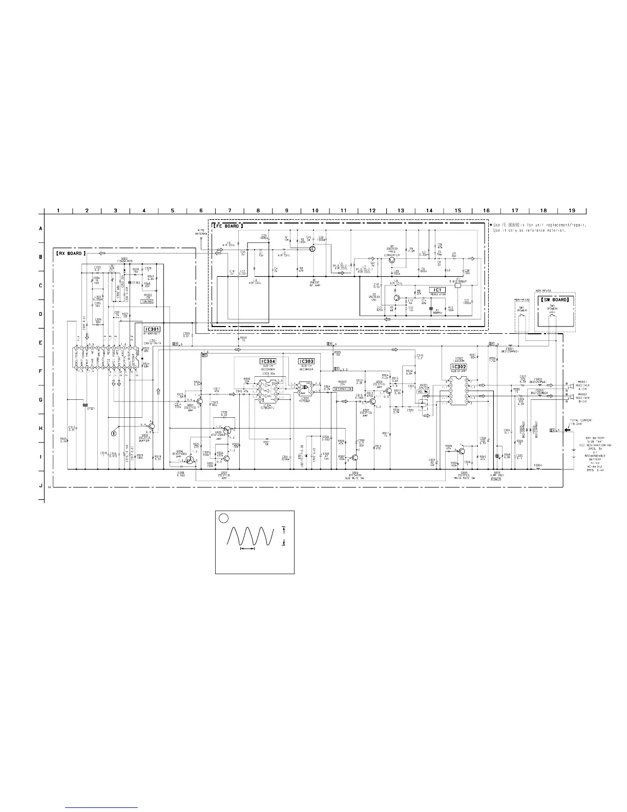
MDR-RF430/RF450
r
Refer to page 6 for IC Block Diagrams.
Note:
• All capacitors are in µF unless otherwise noted. pF: µµF
50 WV or less are not indicated except for electrolytics
and tantalums.
• All resistors are in Ω and
1
/
4
W or less unless otherwise
specified.
•
¢
: internal component.
• U : B+ Line.
• H : adjustment for repair.
• Power voltage is dc 3V and fed with regulated dc power
supply from battery terminal.
• Voltages are dc with respect to ground under no-signal
conditions.
• Voltages are taken with a VOM (Input impedance 10 MΩ).
Voltage variations may be noted due to normal produc-
tion tolerances.
• Waveforms are taken with a oscilloscope.
Voltage variations may be noted due to normal produc-
tion tolerances.
• Circled numbers refer to waveforms.
• Signal path.
F
r
WAVEFORM
1
IC301 @¡
VOLT/DIV : 2m V AC
TIME/DIV : 20 µsec
10mVp-p
20.4
µ
sec
3-2. SCHEMATIC DIAGRAM