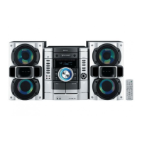
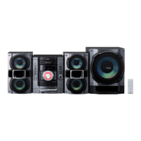
HCD-GX355/GX555/RG270/RG475/RG575
55
HCD-GX355/GX555/RG270/RG475/RG575
• Note For Printed Wiring Boards and Schematic Diagrams
• Indication of transistor
Note on Schematic Diagram:
• All capacitors are in µF unless otherwise noted. (p: pF)
50 WV or less are not indicated except for electrolytics
and tantalums.
• All resistors are in Ω and
1
/
4
W or less unless otherwise
specified.
• f : internal component.
• 2 : nonflammable resistor.
• 5 : fusible resistor.
• C : panel designation.
• A : B+ Line.
• B : B– Line.
• Voltages and waveforms are dc with respect to ground
under no-signal conditions.
– CD Board –
no mark :CD PLAY
– MAIN Board –
no mark : FM
(): CD PLAY
〈〈 〉〉 : TAPE PLAY
[]: REC
∗ : Impossible to measure
• Voltages are taken with a VOM (Input impedance 10 MΩ).
Voltage variations may be noted due to normal produc-
tion tolerances.
• Waveforms are taken with a oscilloscope.
Voltage variations may be noted due to normal produc-
tion tolerances.
• Circled numbers refer to waveforms.
• Signal path.
F : TUNER (FM/AM)
E : TAPE PLAY (DECK-A)
d : TAPE PLAY (DECK-B)
G : REC
J : CD PLAY
f : AUX IN
N : MIC
• Abbreviation
CND : Canadian model
E2 : 120 V AC area in E model
E51 : Chilean and Peruvian models
EE : East European model
RU : Russian model
Note on Printed Wiring Board:
• X : parts extracted from the component side.
• Y : parts extracted from the conductor side.
• f : internal component.
• : Pattern from the side which enables seeing.
(The other layers' patterns are not indicated.)
Caution:
Pattern face side: Parts on the pattern face side seen from
(Conductor Side) the pattern face are indicated.
Parts face side: Parts on the parts face side seen from
(Component Side) the parts face are indicated.
Note:
The components identi-
fied by mark 0 or dotted
line with mark 0 are criti-
cal for safety.
Replace only with part
number specified.
Note:
Les composants identifiés par
une marque 0 sont critiques
pour la sécurité.
Ne les remplacer que par une
pièce portant le numéro
spécifié.
C
B
These are omitted.
E
Q
B
These are omitted.
CE
Q
– MAIN Board –
3
IC201 u; (RFACO)
(CD play mode)
200 mV/DIV, 500 ns/DIV
0.5 to 1.3 Vp-p
22.8 µs
3.3 Vp-p
1
IC201 1 (LRCK), 2 (LRCKI)
(CD play mode)
1 V/DIV, 10
µ
s/DIV
2
IC201 5 (BCK), 6 (BCKI)
(CD play mode)
1 V/DIV, 200 ns/DIV
472 ns
3.3 Vp-p
4
IC201 <z/, (XTAO)
(CD play mode)
1 V/DIV, 20 ns/DIV
59.4 ns
2.3 Vp-p
ws
IC901 qd (XOUT (16MHZ))
500 mV/DIV, 20 ns/DIV
62.2 ns
1 Vp-p
wd
Q201 (Collector)
(REC mode)
500 mV/DIV, 10
µ
s/DIV
17.2 µs
17.6 Vp-p
wa
IC901 qa
(XCOUT (32.768KHZ))
1 V/DIV, 10
µ
s/DIV
30.6 µs
2.8 Vp-p
• Waveforms
– CD Board –
3. DIAGRAMS
 Loading...