Do you have a question about the Sony ta-ve170 and is the answer not in the manual?
Key conventions and notes for interpreting circuit diagrams and printed wiring boards.
Physical layout of the main section's printed wiring board.
Electrical schematic for the main section (part 1).
Electrical schematic for the main section (part 2).
Physical layout of the panel section's printed wiring board.
Electrical schematic for the panel section.
Physical layout of the power supply section's printed wiring board.
Electrical schematic for the power supply section.
Detailed pin assignments and functions for integrated circuits.
Exploded view of the case and front panel, listing parts.
Exploded view of the chassis, listing parts.
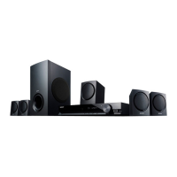
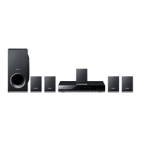
| Brand | Sony |
|---|---|
| Model | ta-ve170 |
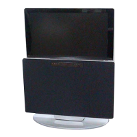
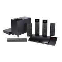
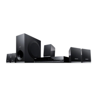
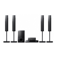
| Category | Home Theater System |
| Language | English |