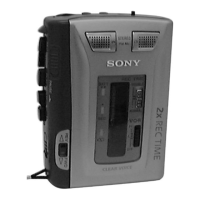
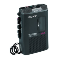
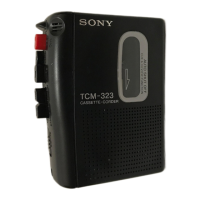
TCS-60DV
— 15 — — 16 — — 17 — — 18 — — 19 —
5-3. PRINTED WIRING BOARD – MAIN SECTION –
12
A
B
C
D
E
F
G
3456789101112131415161718192021222324
Note on Printed Wiring Board:
• X : parts extracted from the component side.
• Y : parts extracted from the conductor side.
• Through hole is omit.
• b : Pattern from the side which enables seeing.
Caution:
Pattern face side: Parts on the pattern face side seen from
(SIDE A) the pattern face are indicated.
Parts face side: Parts on the parts face side seen from
(SIDE B) the parts face are indicated.
Ref. No. Location
D301 B-2
D302 B-20
D303 C-23
D304 C-22
D305 E-13
D306 C-20
D307 B-3
D308 C-9
D701 B-9
D702 B-14
IC101 A-5
IC201 B-17
IC301 D-6
IC303 B-3
IC304 B-19
IC305 D-18
IC501 A-15
IC601 E-14
IC701 C-14
IC702 B-15
Q101 C-6
Q201 B-6
Q301 D-4
Q302 A-19
Q303 B-18
Q304 C-3
Q305 C-2
Q306 B-2
Q307 D-22
Q308 A-1
Q501 B-15
Q502 C-6
Q503 B-7
Q601 D-11
Q602 E-11
Q603 D-11
Q604 C-11
Q701 B-15
Q702 B-9
Q703 D-15
Q704 C-15
Q705 B-13
Q706 B-13
Q707 D-14
Q708 B-7
• Semiconductor
Location