74 Circuit Descriptions TM8100/TM8200 Service Manual
© Tait Electronics Limited June 2006
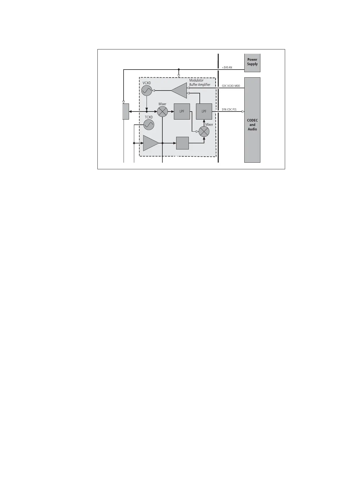
Reference
Frequency
The approximately 25kHz (30kHz for A4) reference is obtained by dividing
the approximately 13MHz (2.612kHz for A4) output of the FCL. Any error
in the FCL output frequency will be multiplied by the synthesizer.
Therefore, if the synthesizer is locked but not the FCL, then the synthesizer
output frequency will be wrong. The FCL frequency division is performed
by a digital counter inside the PLL IC. The divider setting is constant.
VCO Frequency and
Output Power
The output frequency from the synthesizer is generated by a VCO.
The VCO frequency is tuned across the frequency range of the radio by
means of a DC control voltage, typically between 2V and 12V. The VCO
output power is amplified by a buffer amplifier. The power is low and varies
from band to band. The buffer output power depends on which mode—
receive or transmit—is used. In receive mode the output power should be
about 7dBm, whereas in transmit mode it should be about 9dBm.
Dual VCOs Some variants of the synthesizer use two VCOs: one for receive and one for
transmit. Synthesizers with two VCOs share the same tuning signal.
Only one VCO is switched on at a time, and so the PLL IC will see only
one output frequency to tune. A portion of the RF output from the VCOs
is fed to the RF input of the PLL IC. The RF signal is divided by an integer
that gives 25kHz (30kHz for A4) if the output frequency is correct.
Phase-locked Loop The PLL IC compares the 25kHz reference (30kHz for A4) and the divided
VCO signal, and the error is used to control the internal charge pump.
The charge pump is a current source that can sink or source current in
proportion to the frequency or phase error. The output is a series of 25kHz
pulses (30kHz for A4) with a width that is dependent on the phase error.
When the output frequency of the synthesizer is correct, there is no error
and the charge pump output will become open circuit.
Figure 3.6 Block diagram of the frequency control loop circuitry—A4 band
÷ 4
Buffer
Amplifier
FCL
÷ 4
Buffer
Amplifier
FCL
 Loading...