2005/03/29
33
Pin
No.
Pin Name Function Interface Circuit I/O Signal
47 YC Vcc 5V
Vcc terminal for Y/C circuit.
Supply 5V.
⎯ ⎯
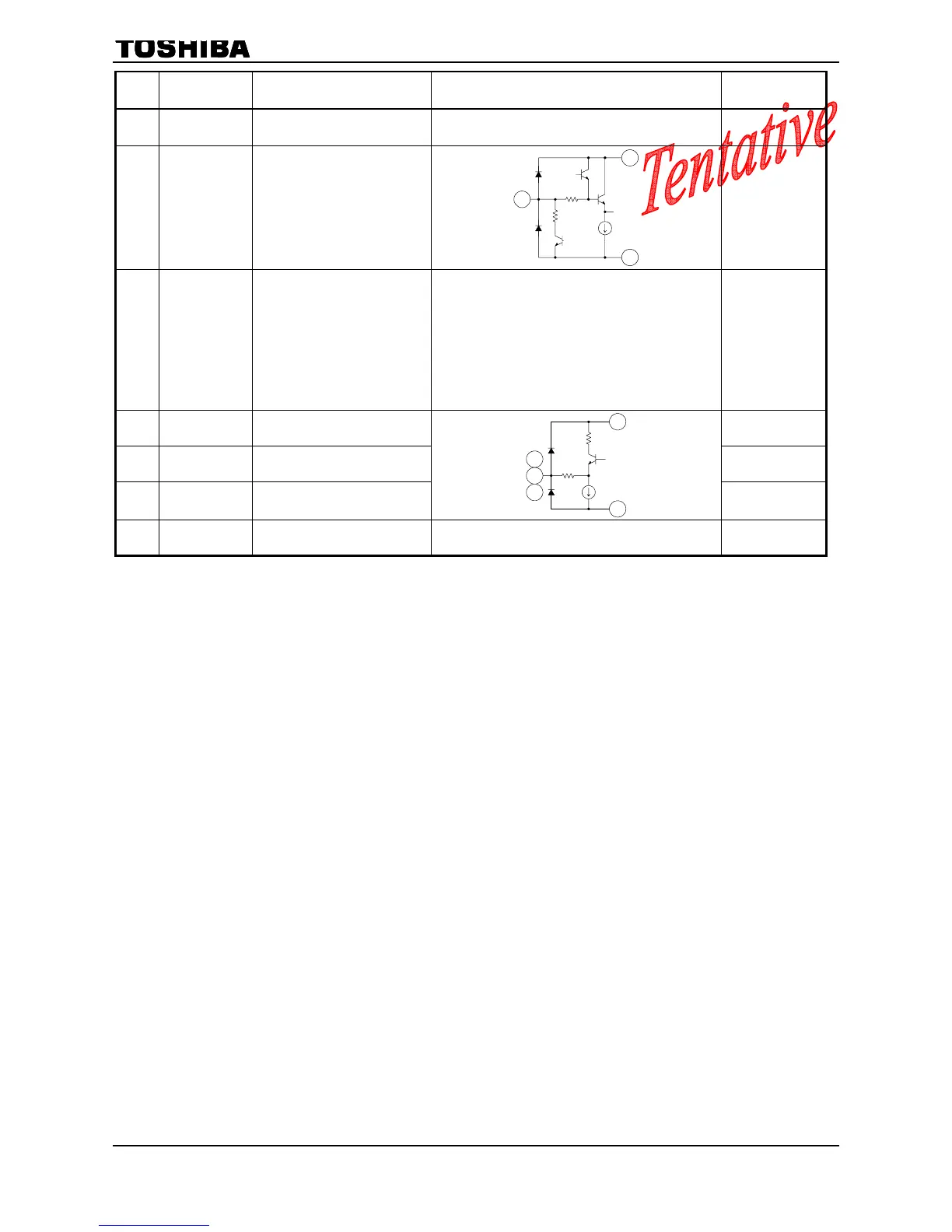
48 Sync out
Output terminal for Sync
pulse.
A pull up resister is required
because of its open
collector output.
(Pull up resister: minimum
4.7kohm)
11
17
48
100Ω
5kΩ
49 DVCC
Vcc terminal for Digital
block.
This terminal voltage is
clipped about 3.3V by
regulator circuit.
Supply DVCC voltage from
A VCC 8V(#17) voltage via
270Ω.
⎯ ⎯
50 R out
Output terminal for R signal.
51 G out
Output terminal for G
signal.
52 B out
Output terminal for B signal.
17
18
51
50
52
100Ω
53 TV DGND
GND terminal for digital
block.
⎯ ⎯
 Loading...