Theory of Operation-2225 Service
Power Supply Probe Adjust
The Power Supply provides the necessary operating
A front-panel PROBE ADJUST output is provided for
voltages for the instrument. Operating potentials are use in adjusting probe compensation. The voltage at
obtained from a circuit consisting of the Power the PROBE ADJUST terminal is a negative-going
Transformer, Pre-regulator, lnverter and multi- square wave that has a peak-to-peak amplitude of
winding transformer. The voltage produced by the approximately 0.5 V with a repetition rate of
Power Transformer output winding, after rectifi- approximately
1
kHz.
cation, provides 45 Vdc minimum to the 40-kHz
Preregulator circuit, which in turn, supplies a
nominal 38 Vdc to the
20
kHz Inverter stage. A High
Voltage Multiplier circuit produces the accelerating,
focus, and cathode potentials used by the crt.
DETAILED CIRCUIT DESCRIPTION
VERTICAL
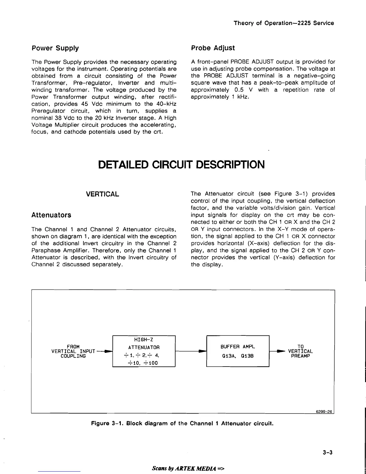
The Attenuator circuit (see Figure 3-1
)
provides
control of the input coupling, the vertical deflection
factor, and the variable
volts/division gain. Vertical
Attenuators
input signals for display on the crt may be con-
nected to either or both the CH
1
OR
X and the CH
2
The Channel
1
and Channel
2
Attenuator circuits,
OR
Y input connectors. In the X-Y mode of opera-
shown on diagram
1,
are identical with the exception
tion, the signal applied to the CH 1
OR
X connector
of the additional Invert circuitry in the Channel
2
provides horizontal (X-axis) deflection for the dis-
Paraphase Amplifier. Therefore, only the Channel
1
play, and the signal applied to the CH
2
OR
Y
con-
Attenuator is described, with the lnvert circuitry of nector provides the vertical (Y-axis) deflection for
Channel
2
discussed separately.
the display.
ATTENUATOR
t-i
BUFFER AMPL
VERTICAL INPUT
COUPLING
,
I.
+
2.e
4,
QI~A,
a138
vmid8L
HIGH-Z
Figure
3-1.
Block diagram of
the
Channel
1
Attenuator circuit.
7
Scans
by
ARTEK
MEDL4
=r,
 Loading...