The Second Amplifier and Driver C.F. stage.
The push-pull output from the Input Amplifier
stage is amplified in the Second Amplifier and
coupled through the Driver C.F. stage to the
Output Amplifier. As mentioned previously, the
positive feedback from the plate circuit on one
side of the amplifier to the grid circuit on the
other makes this stage an infinite gain amplifier.
However, the amplifier does not oscillate due to
the overall negative feedback.
The .2 MV/CM GAIN ADJ. control R456, lo
cated between the two cathodes, sets the small-
signal gain of the Vertical Amplifier. This control
is most effective when the SENSITIVITY switch is
in the 200 /.VOLTS PER CM position. The FEED
BACK BAL. control R455 balances the negative
feedback from both sides of the Driver C.F.
stage; this control is also most effective when the
SENSITIVITY switch is in the 200 /.VOLT PER CM
position.
The Driver C.F. is the load for the Second Am
plifier. Its grid circuit provides the necessary
high impedance with low capacitance to main
tain the gain of the Second Amplifier; its cathode
circuit provides a very low impedance to drive
the input capacitance of the Output Amplifier.
The low output impedance of the cathode circuit
also provides an excellent point from which to
obtain the negative feedback for the Input Am
plifier stage.
The Output Amplifier.
The Output Amplifier is the stage that drives
the vertical-deflection plates in the crt. The gain
of this stage can be adjusted by means of the .2
V/CM GAIN ADJ. control R488. This control is
most effective when the SENSITIVITY switch is
in the .2 VOLTS PER CM position. The variable
capacitor C489 adjusts the high-frequency re
sponse of the amplifier, and is used principally
to provide a constant output capacitance.
By means of the HORIZ. DEF. PLATE SELEC
TOR switch SW489 the Upper-Beam Vertical Am
plifier can be connected to the horizontal-deflec
tion plates in the crt. With this configuration the
instrument can be used as a single-beam X-Y
oscilloscope. The GAIN ADJ. control R489 is
used to increase the gain of the Amplifier slight
ly, necessary for this application.
Trigger Pickoff
When internal triggering of the Time-Base
Generator is desired (TRIGGER SELECTOR in
either of the UPPER or LOWER positions) a
sample of the vertical-output signal is used to
develop the triggering pulse. This sample, ob
tained from the plate circuit of V484B, is coupled
through a frequency-compensated voltage di
vider to V493, a cathode-follower which drives
the Time-Base Trigger circuitry. The INT. TRIG.
DC LEVEL ADJ. control R495 is adjusted to set
the cathode voltage to zero when triggering in
the DC mode and with the beam positioned at
its respective zero-center graticule line.
TIME-BASE TRIGGER
The Time-Base Trigger circuit consists of a trig
gering-signal amplifier V24 and a rectangular-
pulse multivibrator (Schmitt Trigger) circuit V45.
The function of the trigger circuitry is to produce
a negative-going rectangular pulse at the plate
of V45B whose repetition rate is the same as
that of the triggering signal. This negative step
is then differentiated to produce a very sharp
negative spike (trigger) to trigger the Time-Base
Generator in the proper time sequence. A posi
tive spike is also produced by the differentiation
process, but this spike is not used.
The signal from which the rectangular output
is produced may emanate from one of four
sources. When the TRIGGER SELECTOR switch is
in the LINE position, a 6.3-volt signal at the
power line frequency is used for this application.
When the switch is in the UPPER or LOWER posi
tion (AC or DC), the signal is obtained from Up
per- or Lower-Beam Vertical Amplifier, respec
tively. In the EXT position (AC or DC), the signal
is obtained from an external source through a
front-panel connector (TRIGGER INPUT). In any
of the DC positions of the TRIGGER SELECTOR
switch the signal is coupled directly from its
source to the Slope switch SW20. In any of the
AC positions, the signal is coupled through CIO.
Although the output of the Trigger Multi is
always a negative rectangular pulse, the start of
the pulse may be initiated by either the rising
(positive-going) or falling (negative-going) por
tion of the triggering signal. To see how this is
accomplished the operation of the Trigger Multi
will be described first.
In the quiescent state, that is, ready to receive
a signal, V45A is conducting and its plate volt-
4-4
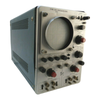
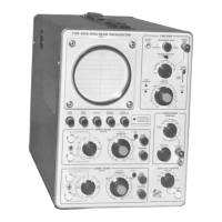
CIRCUIT DESCRIPTION — TYPE 502
 Loading...