Circuit
Description—
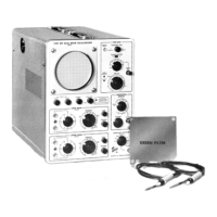
5103N
taining
a steady output.
The output of the supply
is set to
exactly
—30
volts by adjustment
of
R878,
—30
V Adj. This
control sets the
conduction
of
Q870,
which controls the
bias levels
of Q865 and Q860.
CR865 and
Q865
provide
short-circuit
protection by
limiting
the current through
Q860.
+30-Volt Supply.
The
regulator
for
the
+
30-Volt
Supply
consists
of series-pass
transistor Q840 and
error
amplifier
Q850.
This is a
feedback
amplifier system
similar to that
just
described
for the
-30-Volt
Supply.
R858,
+30 V Adj,
provides
an
adjustment to
set
the output of the
supply at
exactly
+30 volts.
Q845
protects
the supply in the event
the output is
shorted by
limiting the current demanded
from the
series-pass
transistor
under excessive
load. During
normal operation,
Q845
is biased
off.
+5-Volt Supply.
The
regulator
for the
+5-Volt
Supply
consists of
series-pass
transistor Q815
and error
amplifier
Q820.
Operation
of this
feedback
amplifier system is
similar to
that
described
for the
-30-Volt Supply.
The
short-protection
transistor,
Q825,
functions as
described
for
Q845
in the
+30-Volt Supply.
Line Trigger
A
line-frequency
signal
is
obtained
from
the
secondary
of
T801
and
attenuated
by R830,
R832,
and R834 to
pro-
vide a
line-trigger
source
for
the
time-base
plug-in unit.
CRT Heater Windings
Two separate secondary windings are
provided
for
the
CRT
writing-gun heaters
and the flood-gun heaters. The
writing-gun heaters are elevated
to
—3500
volts in the
CRT
circuit (display unit)
to maintain a potential near that of
the
CRT cathode.
Calibrator
The
Calibrator circuit
composed
of
Q885, Q890,
and
their
associated
passive
components
produces
a
square-wave
output
with accurate amplitude and
at
a
rate of twice the
power-line frequency. This output is available
at
the probe
test loop on the display unit
front
panel
as a
4-milliampere
(peak to peak) square-wave
current, or
as a
400-millivolt
(ground to peak) square-wave voltage.
The
resistive-capacitive
network
at the
base of
Q885
receives
a
pulsating
DC voltage
from
full-wave
rectifier
CR835-CR836
and
produces
a
nearly
symmetrical
switching
signal
for
Q885
and
Q890.
As
Q890
is
alternately
switched
on
and
off
at twice
the
line
frequency,
current
through
R890
is
alternately
switched
through
the
transistor
or
through
CR890,
the
probe
test loop,
and
R891,
pro-
ducing
the
required
test
signal.
3-3