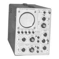
Circuit Description— Type 544/R M544
drops, removing the bias on Q289 and thereby extinguishing
the READY lamp. The runup of the Miller circuit causes the
hold-off multivibrator to switch, and V345A takes control.
NORMAL-SINGLE SWEEP-RESET switch SW135 applies a
positive voltage through D332 to the grid of V345A, and this
positive voltage prevents the holdoff multivibrator from reset
ting until NORMAL-SINGLE SWEEP - RESET switch SW369
has been moved to either the RESET or NORMAL position.
Sweep Timing. The sweep rate (the rate at which the spot
moves across the face of the crt) is determined by the rate
at which the timing capacitor and timing resistor permit the
Miller circuit to run up. By means of TIME/CM switch SW290
(see Timing-Switch schematic), both the size of the capacitor
being charged and the charging current can be selected to
cover a wide range of sawtooth slopes (sweep rates). Note
that SW290 is connected so that switching 8 capacitors and
6 resistors provides 24 different sweep rates, varying from 5
sec/cm to 0.1 ,asec/cm without magnification. The TIME/C M
switch also selects the proper holdoff capacitor and dis
charge resistor for the sweep rate in use.
Continuously variable uncalibrated sweep rates are pro
vided by R290Z and SW290Z (VARIABLE control). When
SW290Z is switched to the UNCAL position, it removes the
short from around R290Z and switches on UNCAL lamp
B290W. By turning VARIABLE control R290Z, the charging
time of the timing capacitor selected by the TIME/CM switch
may be increased by at least 2.5 times the calibrated rate,
providing continuously variable sweep rates.
Horizontal Amplifier
The dc-coupled horizontal amplifier (see Horizontal Ampli
fier schematic) consists of a transistor input amplifier, an
emitter follower, a transistor paraphase amplifier, a push-pull
vacuum-tube output amplifier, a pair of output cathode fol
lowers, and a capacitance-driver tube. In addition, the Type
544 contains a cathode-coupled preamplifier that is used to
amplify externally applied horizontal deflection signals. The
input to the horizontal amplifier is received from the sweep
generator, or the external HORIZ INPUT connector, depend
ing upon the setting of the HORIZONTAL DISPLAY switch
Input Stages. The selected input signal is applied to the
base of Q534 along with dc-positioning voltages from the
horizontal positioning controls. The composite signal output
of Q534 is applied to emitter follower Q543, and from that
transistor to the paraphase amplifier. Negative feedback
from the emitter of Q543 to the base of Q534 keeps the
input and output impedance of the two stages low. R544 (X10
CAL) in the feedback loop provides a means of adjusting
the amount of feedback, thereby providing amplifier gain
adjustment.
Paraphase Amplifier. Q554, Q564 and associated circuit
components form a paraphase amplifier that splits the signal
from Q543 into a push-pull output. The signal from Q554 to
Q564 is coupled through the emitter circuit, and by changing
the value for the coupling resistor, the gain of the paraphase
amplifier is changed to provide sweep magnification. Seven
selectable values of coupling resistor are available providing
XI, X2, X5, XI0, X20, X50, or XI00 sweep magnification.
The feedback loop from the collector of Q554 stabilizes
the gain and balance of the paraphase amplifier. D542 and
D561 provide base-operating bias. The feedback loops from
the output cathode followers (V574B and V584B) to the emit
ters of Q554 and Q564 assist in stabilizing the gain of the
horizontal amplifier.
Output Amplifier and Cathode Followers. The ramp-
voltage outputs of the paraphase amplifier are applied to the
grids of amplifiers V574A and V584A. The ramp voltages
are amplified by the two triodes, which then apply the ramp
voltages to the output cathode followers. To maintain the
desired linearity at high sweep rates, part of the output from
each amplifier is bypassed around the cathode followers
through small variable capacitors C572 and C582. C576 and
C586 together with the stray capacitance across R576 and
R586 form a capacitance bridge to provide correct high-fre
quency feedback.
Capacitance Driver. The cathode of V574B drives the left-
hand deflection plate and, during the sweep, the cathode
voltage should go linearly in a negative direction. At high
sweep rates, when V574B tries to drive the deflection plate
negative, the deflection-plate capacitance and the output
capacitance of cathode follower V574B tend to distort the
ideal linear ramp voltage into an rc discharge curve. To
overcome this tendency toward nonlinearity, the positive
going ramp voltage at the cathode of V584B is applied
through C591 to the grid of capacitance driver tube V589.
The positive-going voltage on the grid of V589 forces it into
heavy conduction, and the current supplied through the tube
provides extra current to the cathode of V574B and helps to
discharge the capacitance in the output of V574B. Since the
crt is blanked during the return trace, there is no need for a
similar current driver at the cathode of V584B.
External Horizontal Preamplifier. The preamplifier ap
plies external horizontal deflection voltages through the
HORIZONTAL DISPLAY switch to the grid of V514B. For
large amplitude signals, XI0 and XI00 attenuator positions
are provided on the HORIZONTAL DISPLAY switch. V514B
and V514A form a cathode-follower grounded-grip amplifier,
with a gain controlled by adjusting the value of the coupling
resistor between the two cathodes. In this case, R511 pro
vides at least a 10:1 range of adjustment. The output of
V514A is applied through the HORIZONTAL DISPLAY switch
to the base of Q534.
Amplitude Calibrator
The amplitude calibrator in the Type 544 is a 1-kc square-
wave generator (see Amplitude Calibrator schematic) that
provides both voltage and a 5-ma current output to the
front-panel connectors. The voltage output is taken from the
CAL OUT connector on the front panel, where either a
selectable-amplitude square wave or a steady + 100-volt
dc reference voltage is available. By turning the AMPLITUDE
CALIBRATOR switch, the amplitude of the square-wave out
put may be varied from 0.2 mvolts to 100 volts, peak-to-peak.
The current output is applied to the 5 ma current strap.
The arrow indicates conventional current flow. When
the AMPLITUDE CALIBRATOR switch is in the 100 VDC
position, the link has 5 ma dc flowing through it; when the
switch is in the 5 mA position, the current through the link is
in the form of a 1-kc, 5 ma square wave.
CAUTION
The link is designed for use with a snap-on current
probe and does not unplug.
3-8
@1
 Loading...