Typical Characteristics
2–26
TDS Family Performance Verification and Specifications
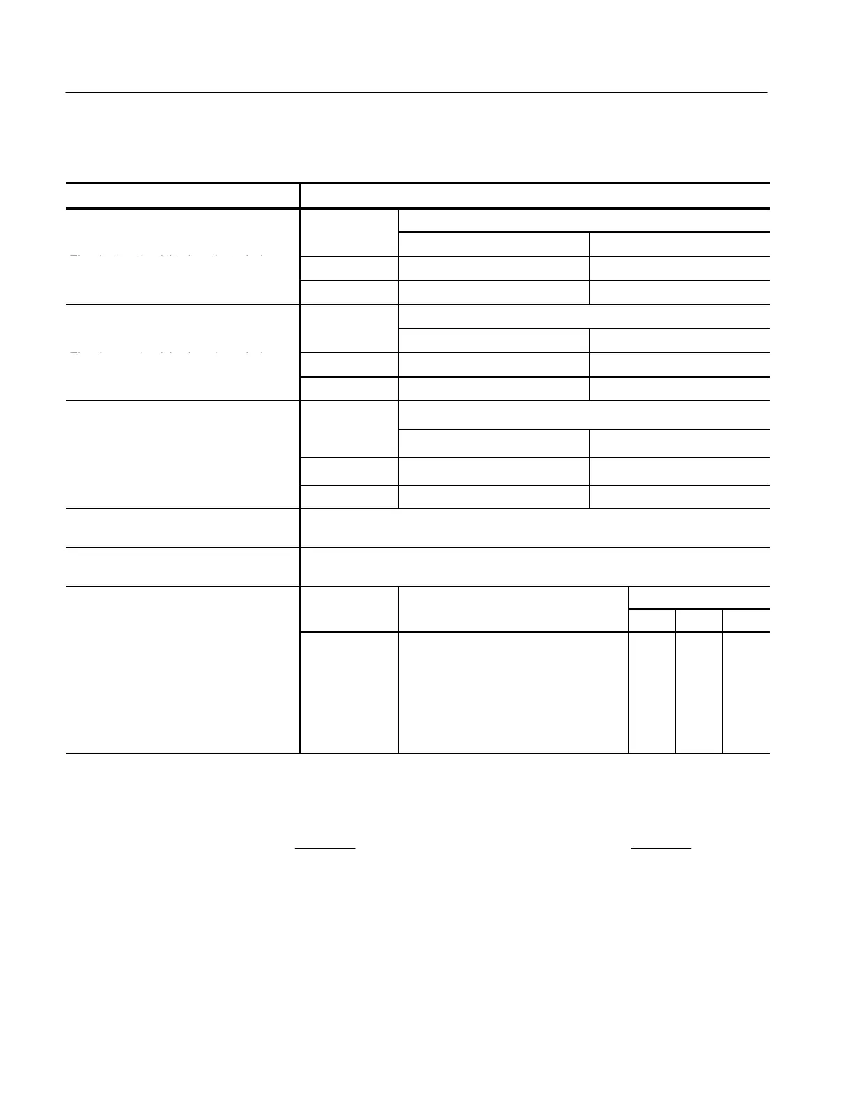
Table 2–15: Typical Characteristics — Signal Acquisition System (Cont.)
Name Description
Effective Bits
— TDS 520B, 724A
Sample Rate
— TDS 520B, 724A
The chart on the right gives the typical
Frequency
1 GS/s 10 MS/s & HiRes
The chart on the right gives the typical
effective bits for a sine wave adjusted to
1 MHz – 9.2 divs 6.8 bits 9.7 bits
effective bits for a sine wave adjusted to
9.2 divisions at 1 MHz, 50 mV/div @ 25° C
500 MHz
6.8 bits N/A
Effective Bits
— TDS 540B, 744A
Sample Rate
— TDS 540B, 744A
The chart on the right gives the typical
Frequency
2 GS/s 10 MS/s & HiRes
The chart on the right gives the typical
effective bits for a sine wave adjusted to
1 MHz – 9.2 divs 6.8 bits 9.7 bits
effective bits for a sine wave adjusted to
9.2 divisions at 1 MHz, 50 mV/div @ 25° C
500 MHz
6.8 bits N/A
Effective Bits — TDS 784A
The chart on the right gives the typical
Sample Rate
The chart on the right gives the typical
effective bits for a sine wave adjusted to
Frequency
4 GS/s 10 MS/s & HiRes
effective bits for a sine wave adjusted to
9.2 divisions at 1 MHz, 50 mV/div @ 25° C
1 MHz – 9.2 divs 6.6 bits 9.7 bits
1 GHz – 6.5 divs 5.5 bits N/A
Frequency Limit, Upper, 250 MHz
Bandwidth Limited
250 MHz
Frequency Limit, Upper, 20 MHz Band-
width Limited
20 MHz
Step Response Settling Errors
Settling Error (%)
3
at
Step Response Settling Errors
Setting
±
20 ns 100 ns 20 ms
1 mV/div – 100
mV/div
101 mV/div –
1 V/div
1.01 V/div – 10
V/div
≤2 V
≤20 V
≤200 V
0.5%
1.0%
1.0%
0.2%
0.5%
0.5%
0.1%
0.2%
0.2%
1
The limits given are for the ambient temperature range of 0_C to +30_C. Reduce the upper bandwidth frequencies by
5 MHz for the TDS 600B or by 2.5 MHz for the TDS 500B/700A for each _C above +30_C.
2
The numbers given are valid 0_C to +30_C and will increase as the temperature increases due to the degradation in
bandwidth. Rise time is calculated from the bandwidth. It is defined by the following formula:
Note that if you measure rise time, you must take into account the rise time of the test equipment (signal source, etc.) that
you use to provide the test signal. That is, the measured rise time (RT
m
) is determined by the instrument rise time (RT
i
)
and the rise time of the test signal source (RTgen) according to the following formula:
TDS 600BRise Time (ns) +
450
BW (MHz)
RT
m
2
+ RT
i
2
) RT
gen
2
TDS 500Bń700ARise Time (ns) +
400
BW (MHz)
3
The values given are the maximum absolute difference between the value at the end of a specified time interval after the
midlevel crossing of the step and the value one second after the midlevel crossing of the step, expressed as a percentage
of the step amplitude.
 Loading...