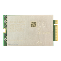
Note: PCIE_RESET_N operates as digital input in PCIe end point mode and open
drain in PCIe root complex mode. PCIE_CLKREQ_N and PCIE_WAKE_N operate as
an open drain in PCIe end point mode, and digital input in PCIe root complex mode.
The default of the FN990 Family is end point mode.
Note: Consider placing a low-capacitance ESD protection component to protect
the FN990 against ESD spikes.
Warning: FN990 data cards are not designed or intended to support Hot-Swap or
Hot-Plug connection. Performing How-Swap or Hot-Plug may pose a danger to the
FN990 Family module, to the host device, and to the person handling the device.
PCIe Layout Guidelines
The below guidelines will provide general guidelines for the PCIe interface to improve
signal integrity.
•
All other sensitive/high-speed signals and circuits must be protected from
PCIe corruption.
•
PCIe signals must be protected from noisy signals (clocks, SMPS, and so
forth).
•
Pay extra attention to crosstalk, ISI, and intralane skew and impedance
discontinuities.
•
PCIe Tx AC coupling capacitors are better placed close to the source or
receiver side to keep good SI of the route on the PCB.
•
To maintain impedance balance, maintain positive and negative traces as
balanced as possible in terms of the signal and its return path.
•
Trace length matching between the reference clock, Tx, and Rx pairs is not
required.
•
External capacitors also should keep differential traces. Ensure not to
stagger the capacitors. This can affect the differential integrity of the design
and can create EMI.
Table 32: PCIe Routing Constraints

 Loading...