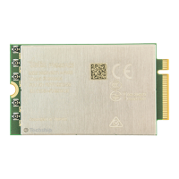
FN990 Family Hardware Design Guide
15 DOCUMENT HISTORY
Table 68: Document History
Enable n12, n13, n14, n18, n26, n29, n76
Conformity section updated (ISED RSS Issues)
Table 1 Applicability Table updated
Added model on Table 1 Applicability Table
Updated Note for Configurations Pins
Updated Note on Section 5.3 Thermal Design Guidelines
Added Note for active high on Section 7.3 SIM interface
Section 12.2 updated with Brazil ANATEL approval
for FN990A28.
Section 12.2 updated with Taiwan NCC approval
for FN990A28.
Updated Table 12: operating temperature range
USB OTG Feature added on Section 7.3.
Updated Section 2.6.1 Conducted Transmit Output Power
Updated Section 3.1 Pin-out
Updated Section 6.3.1 CIe Interface
Updated Section 11.3.2 APAC Approvals
Updated Figure 12: Connection for PCIe Interface
Updated note under section Host Interface
Updated Table 36: I2C Signal
Updated Template
Conformity section updated
Section 2.2.1 Updated Frequency Bands
Section 2.4 Updated Main Features
Section 2.4.1 Updated Configurations Pins
Editorial changes
Minor updates and clarifications throughout all document
Conformity section updated
Maximum antenna gain values added
Some pin-out table descriptions updated
Section 2.2.1 Updated Frequency Bands
Section 2.6 Updated RF Performance
Section 2.4 PCIe Gen 4 -> PCIe Gen 3
Section 3.1 Updated 3.1 Pin-out

 Loading...