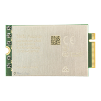
FN990 Family Hardware Design Guide
Section 3.3 Updated 3.3 Pin Layout
Section 4.2 Updated Power consumption
Section 6.3.1.2.1 Added PCIe Layout Guidelines
Section 6.3.1.3.1 Added USB Layout Guidelines
Section 6.4 Updated General Purpose I/O
Section 7.1.1 Updated Antenna Configuration
Section 7.2 Updated Antenna Connector
Section 8.4 Solder Resist Opening Area and Keepout Area added
Section 13. Updated Glossary
Section 6.2 Updated Power ON/OFF/RESET
Section 2.4, 6.3.2, 6.3.3 Updated eSIM description
Section 4.2 Updated Power consumption
Section 2.6.2 Conducted Receiver Sensitivity
Section 2.4 Updated Processor Clock
Section 3.1 Updated Pin-out
Section 3.3 Updated Pin Layout
Section 4.1 Updated Power Supply Requirements
Section 4.2 Updated LPM Power Consumption
Section 6.1 Updated I/O Operating Range
Section 6.2 Updated Power ON/OFF/RESET
Section 6.3 Added and updated information about interfaces

 Loading...