MT8206
PRELIMINARY, SUBJECT TO CHANGE WITHOUT NOTICE MTK CONFIDENTIAL, NO DISCLOSURE
June, 2006
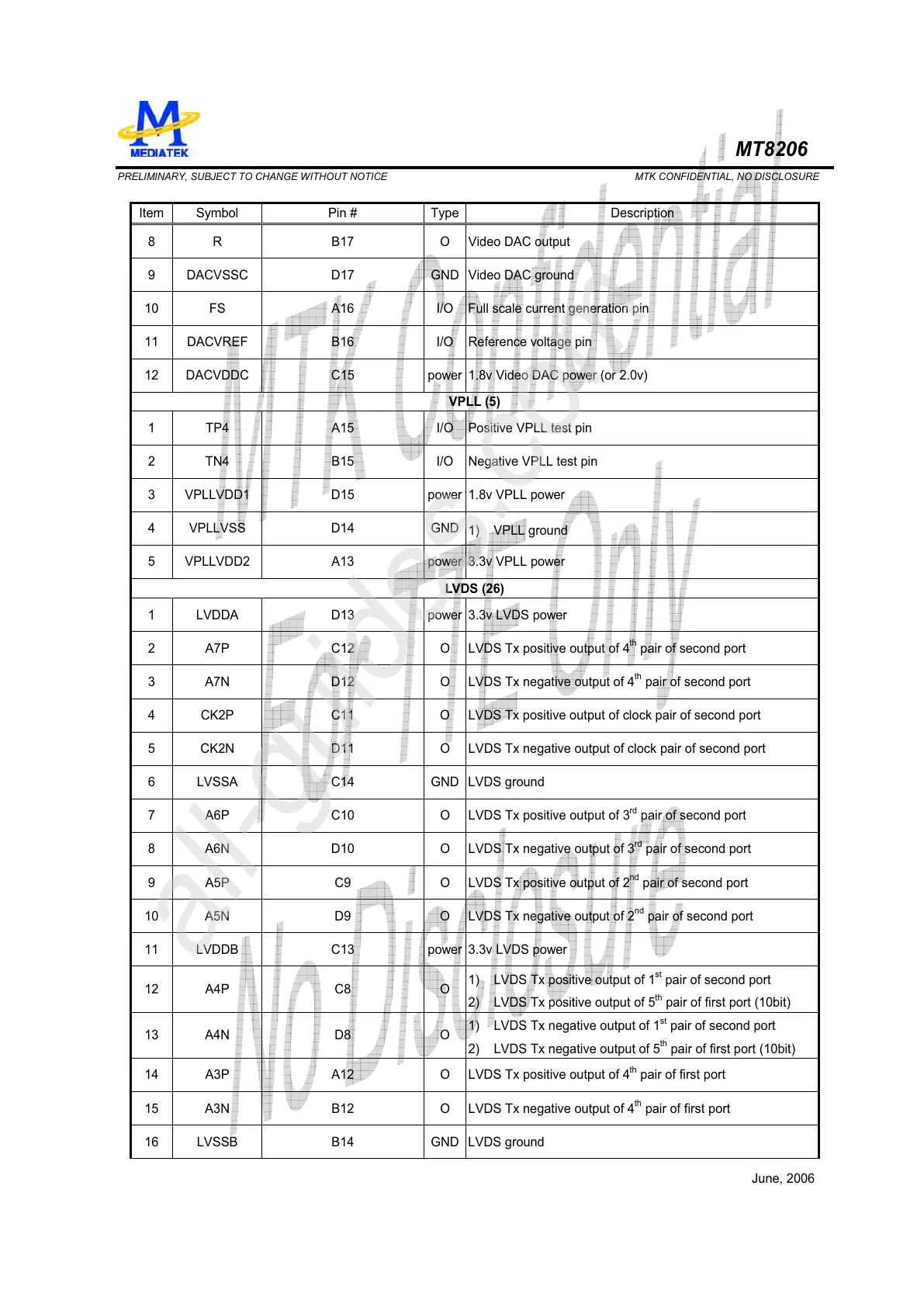
Item Symbol Pin # Type Description
8 R B17 O Video DAC output
9 DACVSSC D17 GND Video DAC ground
10 FS A16 I/O Full scale current generation pin
11 DACVREF B16 I/O Reference voltage pin
12 DACVDDC C15 power 1.8v Video DAC power (or 2.0v)
VPLL (5)
1 TP4 A15 I/O Positive VPLL test pin
2 TN4 B15 I/O Negative VPLL test pin
3 VPLLVDD1 D15 power 1.8v VPLL power
4 VPLLVSS D14 GND
1) VPLL ground
5 VPLLVDD2 A13 power 3.3v VPLL power
LVDS (26)
1 LVDDA D13 power 3.3v LVDS power
2 A7P C12 O LVDS Tx positive output of 4
th
pair of second port
3 A7N D12 O LVDS Tx negative output of 4
th
pair of second port
4 CK2P C11 O LVDS Tx positive output of clock pair of second port
5 CK2N D11 O LVDS Tx negative output of clock pair of second port
6 LVSSA C14 GND LVDS ground
7 A6P C10 O LVDS Tx positive output of 3
rd
pair of second port
8 A6N D10 O LVDS Tx negative output of 3
rd
pair of second port
9 A5P C9 O LVDS Tx positive output of 2
nd
pair of second port
10 A5N D9 O LVDS Tx negative output of 2
nd
pair of second port
11 LVDDB C13 power 3.3v LVDS power
12 A4P C8 O
1) LVDS Tx positive output of 1
st
pair of second port
2) LVDS Tx positive output of 5
th
pair of first port (10bit)
13 A4N D8 O
1) LVDS Tx negative output of 1
st
pair of second port
2) LVDS Tx negative output of 5
th
pair of first port (10bit)
14 A3P A12 O LVDS Tx positive output of 4
th
pair of first port
15 A3N B12 O LVDS Tx negative output of 4
th
pair of first port
16 LVSSB B14 GND LVDS ground