MT8206
PRELIMINARY, SUBJECT TO CHANGE WITHOUT NOTICE MTK CONFIDENTIAL, NO DISCLOSURE
June, 2006
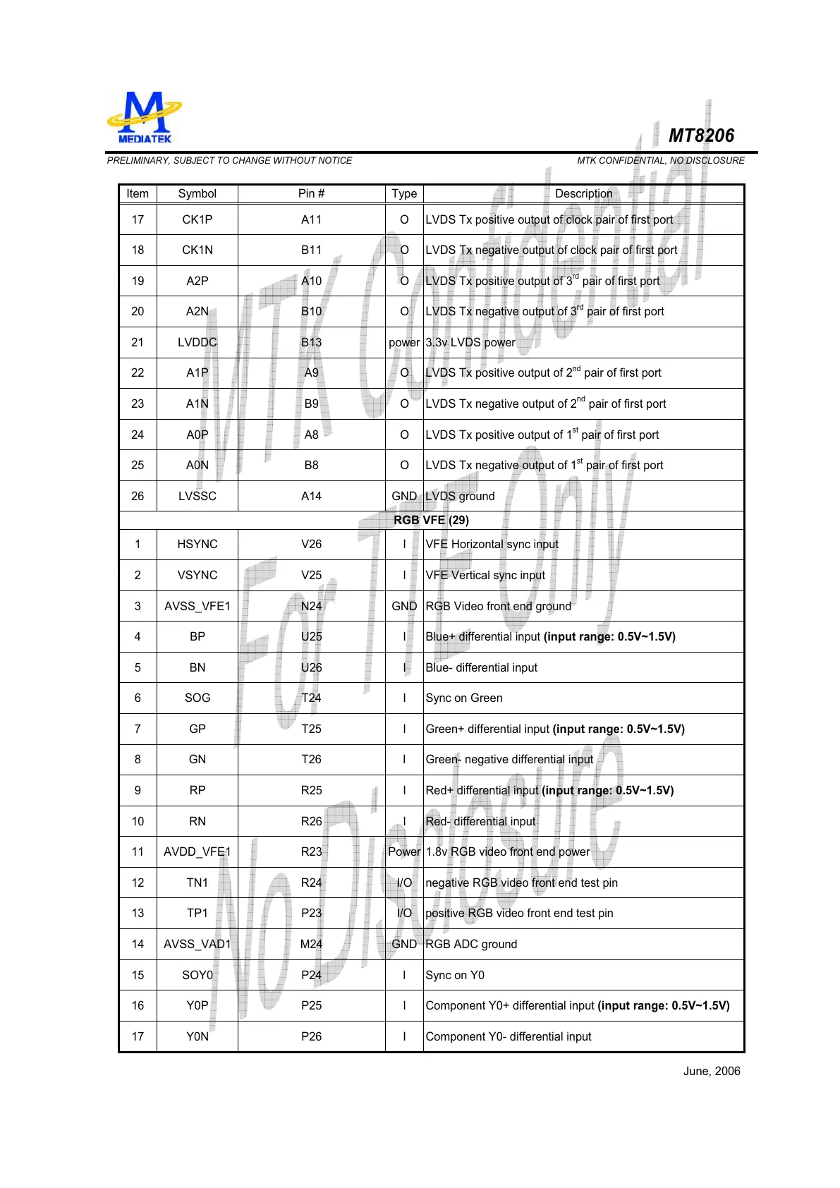
Item Symbol Pin # Type Description
17 CK1P A11 O LVDS Tx positive output of clock pair of first port
18 CK1N B11 O LVDS Tx negative output of clock pair of first port
19 A2P A10 O LVDS Tx positive output of 3
rd
pair of first port
20 A2N B10 O LVDS Tx negative output of 3
rd
pair of first port
21 LVDDC B13 power 3.3v LVDS power
22 A1P A9 O LVDS Tx positive output of 2
nd
pair of first port
23 A1N B9 O LVDS Tx negative output of 2
nd
pair of first port
24 A0P A8 O LVDS Tx positive output of 1
st
pair of first port
25 A0N B8 O LVDS Tx negative output of 1
st
pair of first port
26 LVSSC A14 GND LVDS ground
RGB VFE (29)
1 HSYNC V26 I VFE Horizontal sync input
2 VSYNC V25 I VFE Vertical sync input
3 AVSS_VFE1 N24 GND RGB Video front end ground
4 BP U25 I
Blue+ differential input (input range: 0.5V~1.5V)
5 BN U26 I Blue- differential input
6 SOG T24 I Sync on Green
7 GP T25 I
Green+ differential input (input range: 0.5V~1.5V)
8 GN T26 I Green- negative differential input
9 RP R25 I
Red+ differential input (input range: 0.5V~1.5V)
10 RN R26 I Red- differential input
11 AVDD_VFE1 R23 Power 1.8v RGB video front end power
12 TN1 R24 I/O negative RGB video front end test pin
13 TP1 P23 I/O positive RGB video front end test pin
14 AVSS_VAD1 M24 GND RGB ADC ground
15 SOY0 P24 I Sync on Y0
16 Y0P P25 I
Component Y0+ differential input (input range: 0.5V~1.5V)
17 Y0N P26 I Component Y0- differential input