11
IV. Theory of Operation
For ease of service the MX385 has been designed into 8 replaceable modules. The
modules are:
A. Front Panel Assembly
B. Rear Panel Assembly
C. Computer Board
D. NAV Receiver
E. COMM Receiver
F. NAV Synthesizer
G. COMM Synthesizer
H. Transmitter
A block diagram is shown in drawing AT1900, Top Assembly
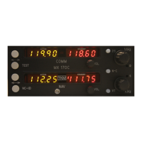
A. Front Panel Assembly (Dwg. SS1930)
The front panel includes the four frequency displays, a photocell for automatic brightness
control, 7 push buttons, two volume controls (the COMM control incorporates the power
switch) and two frequency selection switches. The displays and controls are connected to
the display driver board through pin and socket connectors and to the computer board
with a ribbon cable
.
B. Rear Panel Assembly (Dwgs. SS1945, SS1940)
The rear panel includes the power converter, the audio circuits and T/R switching
circuits.
The audio is amplified in IIA and then selected with Q13. The audio is inverted in IIB
and further amplified in Q3 and Q4. IIC is used to monitor the DC current flowing in Q3
and Q4 and adjust the bias so that the current is 0.20 Adc.
The modulation amplifier consists of I4, Q11 and Q12. Diodes D19 and D20 provide
peak to peak limiting of the microphone input signal to prevent modulation splatter. C2,
C25 and C28 provide high frequency roll-off to prevent adjacent channel interference.
Q2, Q8, Q9, Q10 and Q13 are all used in the T/R switching.
Q15 drives the PIN diode in the T/R switch so that in the transmit mode the drive
impedance is very high and in the receive mode 5 mA of turn-on current is provided.
Q14 is an FET Power Switch controlled by the front panel power switch. When Q1 is
switched on Q1 is also switched on to provide external NAV power.
I3 is a switching regulator that drives Q7 and converts the input line voltage (20 –32 vdc)
to a regulated 5.2 vdc. Q5 and Q6 form a free-running inverter and supply approximately
+20 vdc. The +20 vdc supply is regulated by I2 to provide a stable +15 vdc supply.
The T/R Switch (Dwg. SS1921) contains switching diode D1 and a low pass filter L1,
C2, L2, C3. In receive mode, the diode is forward biased to couple the receiver to the
 Loading...