EasyManua.ls Logo

Vector 4 - Page 206

Vector 4
227 pages
Print Icon
To Next Page IconTo Next Page
To Previous Page IconTo Previous Page
Loading...
¥
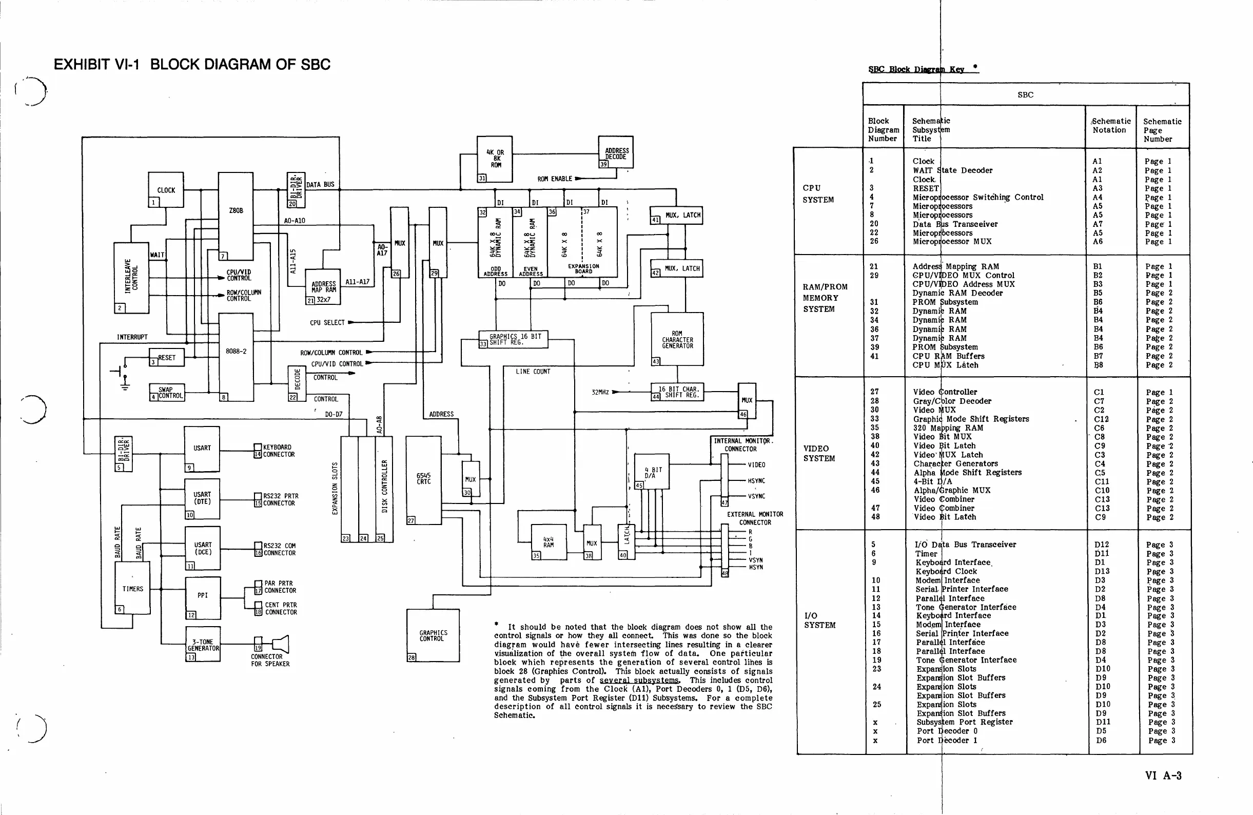
EXHIBIT
VI-1
BLOCK
DIAGRAM
OF
SBC
SBC
Block
Disgrain
Key
*
SBC
Block
Schematic
Schematic
|
Schematic
Diagram
Subsysfiem
Notation
Page
Number
Title
Number
ADDRESS
’
0
m;%%R
3QDEC°DE
1
Clock
Al
Page
1
2
WAIT
State
Decoder
A2
Page
1
o
.
31]
ROM
ENABLE
————-'
Clock.
Al
Pege
1
cLoCK
&5
|DATA
BUS
CPU
3
RESET
Ai
Page
i
=
4
Microprocessor
Switching
Control
A
Page
1]
)
DI
DI
Dl
o
SYSTEM
7
Microprocessors
'
A5
Page
1
2608
32
34]
36]
13
:
L]
MUX,
LATCH
8
Mieroprjocessors
A5
Pege
1
AO-A10
=
z
i
'
i
20
Data
Bus
Transceiver
AT
Page
1
w0
0o
©
i
o 22
Mieroprbeessors
A5
Page
1
<E
=<E
<
b
o
26
Microprocessor
MUX
A6
Page
1
AQ-
MuX
MUX
.
-
=
~
:
>
WAIT
_dfl
2
I
A7
—
25
2a
2
:
®
21
Address
Mapping
RAM
Bl
Page
1
s
-
EXPARS
|
ON
MUX,
LATCH
res
apping
a8
CONTROL
<
|z
23
ADDRESS
|
ABDRESS
BOARD
l
22
29
GPU/VIDEO
Mde
Cont%c;%
gg
gage
i
G2
-
-
CPU/VIDEO
Address
M
age
Wz
ADDRESS
|
A11-A17
Do
DO
00
40
RAM/PROM
:
=5
o
ROW/COLUMN
MAP RAY
;
MEMORY
Dynamic
RAM
Decoder
gg
gage
g
™"
CONTROL
21)
32x7
‘
SYSTEM
31
PROM
u%sx;ltem
Ba
P%Z
2
2
]
32
Dynami
]
34
Dynami¢
RAM
B4
Page
2
CPU
SELECT
»=—
o
36
Dynamif
RAM
B4
gge
2
|
GRAPHICS
16
BIT
HARACTER
37
Dynamie
RAM
B
e
e
33]
SHIFT
REG.
|
CENERATOR
39
PROM
Subsystem
B6
Page
2
8088-2
RON/COLUMN
CONTROL
®-
41
CPU
RAM
Buffers
B7
Page
2
e
CPU/VID
CONTROL
™
—
43
CPU
MUX
Lateh
:
B8
Page
2
8
p——
—i
1
S
[
CONTROL
i
'i
=
a
16
BIT
CHAR.
27
Video
Controller
C1
Page
1
=
SWAP
=
32MHZ
B——i——
@
8
22]
CONTROL
2]
SHIFT
REG.
MUX
28
Gray/Color
Decoder
C7
que
2
.
30
Video
MUX
C2
Page
2
bo-07
%
ADDRESS
1
33
Graphic
Mode
Shift
Registers
.
gfliz
lI;age
g
!
:
35
320
Mapping
RAM
age
o
0
=
‘
38
Video
Bit
MUX
"
C8
Page
2
e
INTERRAL
HORTTOR
VIDEO
40
Video
Bit
Latch
C9
Page
2
=~
USART
[]KEYBOARD
‘
'
CONNECTOR
a0
h
C3
Page
2
E
14}
CONNECTOR
]
SYSTEM
42
Video*MUX
Late
e
Pag
:
ma
»
o
:
VIDEO
43
Character
Generators
age
5]
|
5]
5
=
|
ou
44
Alpha
Mode
Shift
Registers
Cs5
Page
2
%
2
G4z
MUX
[
-
HSYNC
45
4-Bit
D/A
c11
Page
2
5 5
v
L3
-
46
Alpha/Graphic
MUX
C10
Page
2
USART
]Rs232
PRTR
2
©
=
—
VSYNC
Video
Combiner
C13
Page
2
(OTE)
l
CONNECTOR
g
4
+
;
-
47
Video
Gombiner
C13
Pege
2
1o
&
=
'
;
EXTERNAL
MONITOR
48
'Video
Bit
Lateh
c9
Page
2
27
:
CONNECTOR
|
wl
L
R
5
&
23]
[73]
[25
iyt
—EG
]
.
o=
'
D12
Page
3
al
A
USART
IRS232
COM
RAM
B
5
/0
Data
Bus
Transcelver
21t
Pag
;
z
=2
(DCE)
[T6]
CONNECTOR
m
1
6
Timer
age
o
=
]
VSYN
9
Keybodrd
Interface,
D1
Page
3
1
n
HSYN
Keybogrd
Clock
D13
Page
3
10
Modem|
Interface
D3
Page
g
[
]
PAR
PRTR
11
Serial
[Printer
Interface
D2
Page
TIMERS
PP
COMNECTOR
——
'
12
Paralldl
Interface
D8
Page
3
"]
CENT
PRTR
13
Tone
(renerator
Interface
D4
Page
3
6
18]
CONNECTOR
/0
14
Keybogrd
Interface
)
Page
3
=
/
4
terf
D3
Page
3
I
*
It
should
be
noted
that
the
block
diagram
does
not
show
all
the
SYSTEM
15
Modem,
Interface
;
ge
3
GRAPHICS
:
:
16
Serial
{Printer
Interface
D
Page
CONTROL
control
signals
or
how
they
all
connect.
This
was
dope
S0
the
block
17
Paralld]
Interface
D8
Page
3
3-TONE
‘
diagram
would
havé
fewer
intersecting
lines
resulting
in
a
clearer
18
Parallél
Interface
D8
Page
3
GENERATOR
o
CTon
=
visualization
of
the
overall
system
flow
of
data,
One
pafticular
19
Tone
Generator
Interface
D4
Page
3
13
FOR
SPEAKER
block
which
represents
the
generation
of
several
control
lines
is
93
Expansion
Slots
D10
Page
3
block
28
(Graphics
Control).
This
block
actually consists
of
signals
Expa
ion
Slot
Buffers
D9
Page
3
generated
by
parts
of
several
subsystems.
This
includes
control
pansi
.
0 3
;
p
>
24
Expandion
Slots
D1
Page
signals
coming
from
the
Clock
(Al),
Port
Decoders
0,
1
(D5,
D6),
Fxnandion
Slot
Buffers
D9
Page
3
and
the
Subsystem
Port
Register
(D.l‘l)_
Subsystems.
For'a
complete
25
Expa
ion
Slots
D10
Page
2
description
of
all
control
signals
it
is
necessary
to
review
the
SBC
Exga
ion
Slot
Buffers
D9
Page
3
Schematic.
X
Subsystem
Port
Register
D11
Page
3
X
Port
Lecoder
0
D5
Page
3
X
Port
Decoder
1
D6
Page
3
¢
VI
A-3