EasyManua.ls Logo

Vector 4 - Page 207

Vector 4
227 pages
Print Icon
To Next Page IconTo Next Page
To Previous Page IconTo Previous Page
Loading...
EXHIBIT
VI-2
(A)
SCHEMATIC
OF
SBC
SBC
Schematic
Key
.
=1
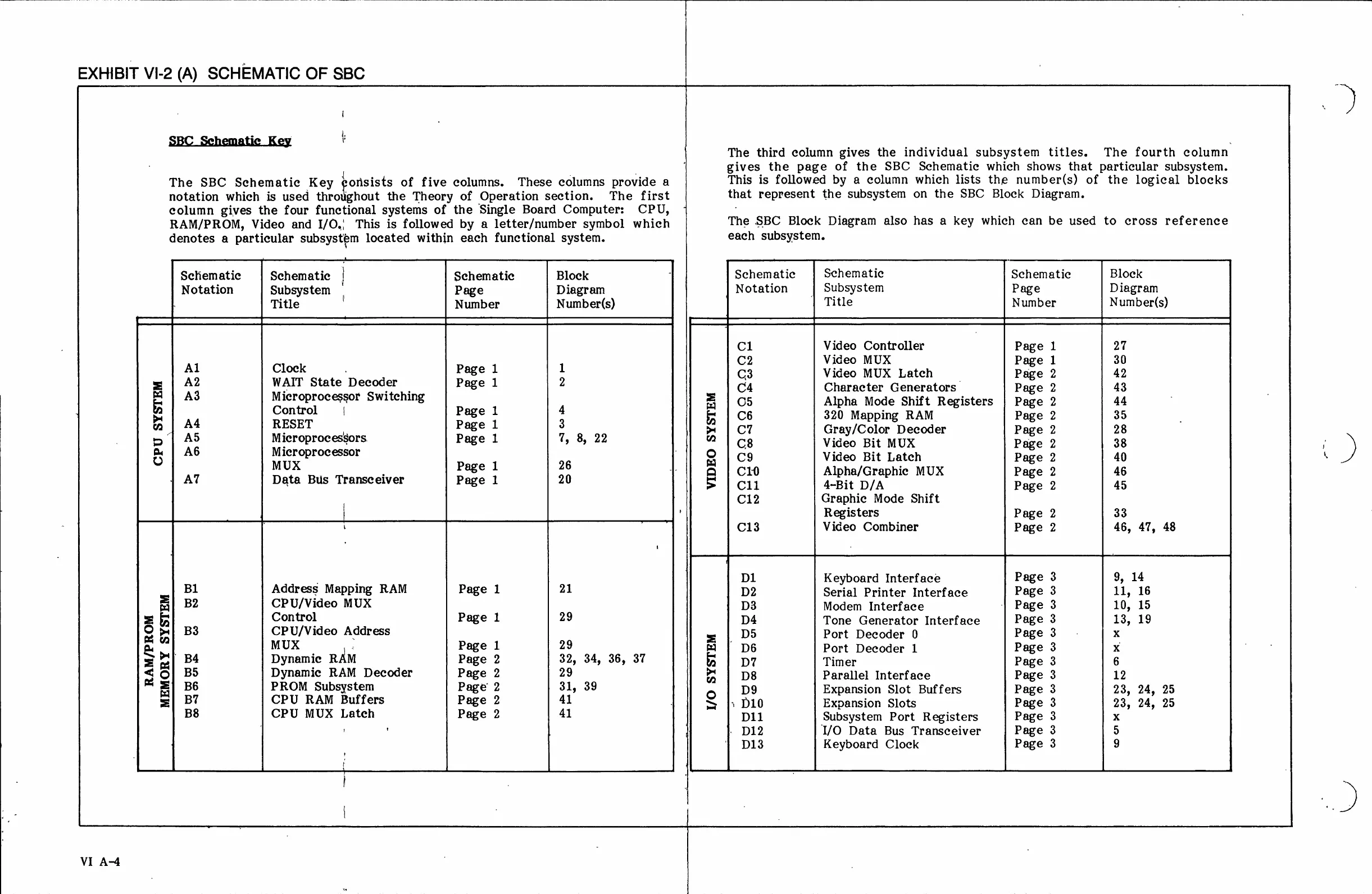
The
SBC
Schematic
Key
ffonsists
of
five
columns.
These
columns
provide
a
notation
which
is
used
throughout
the
Theory
of
Operation
section.
The
first
column
gives
the
four
functional
systems
of
the
Single
Board
Computer:
CPU,
RAM/PROM,
Video
and
I/O.,
This
is
followed
by
a
letter/number
symbol
which
denotes
a
particular
subsystem
located
within
each
functional
system.
The
third
eolumn
gives
the
individual
subsystem
titles.
gives
the
page
of
the
SBC
Schematic
which
shows
that
particular
subsystem.
This
is
followed
by
a
column
which
lists
the
number(s)
of
the
logical
blocks
that
represent
the
subsystem
on
the
SBC
Block
Diagram.
The
SBC
Block
Diagram
also
has
a
key
which
can
be
used
to
cross
reference
each
subsystem.
The
fourth
column\
Schematic
Schematie
§
Schematic
Block
Schematic
Schematic
Schematic
Block
Notation
Subsystem
Page
Diagram
Notation
Subsystem
Page
Diagram
Title
?
Number
Number(s)
Title
Number
Number(s)
C1
Video
Controller
Page
1
27
C2
Video
MUX
Page
1
30
::;
VCJIAOI?II‘(
StatebDecoder
gage
i
%
G3
Video
MUX
Latch
-
Page
2
12
=
A3
Microprocessor
Switehin
age
C4
Character
Generators
Page
2
43
E
Cont?‘[t))
1
g
p
1
1
E
CS
Alpha
Mode
Shift
Registers
|
Page
2
44
M
|
4y
RESET
age
3
&2
|
Cs
320
Mapping
RAM
Page
2
35
@
.
L
Page
1
>
|
C7
Gray/Color
Decoder
Page
2
28
5|
AS
Microprocessors.
Page
1
7
8,
22
2
|
g
Video
Bit
MUX
Page
2
38
&
|
A6
Mieroprocessor
o
‘
Video
Bit
Latch
p
9
40
O
MUX
Pace
1
26
R
C9
ldeo
Bit
Late
age
AT
D
./
.
ag
a
|
cro
Alpha/Graphic
MUX
Page
2
46
ata
Bus
Transceiver
Page
1
20
5
|
c11
4-Bit
D/A
Page
2
45
C12
Graphic
Mode
Shift
4
Registers
Page
2
33
‘
\
C13
Video
Combiner
Page
2
46,
47,
48
.
)
D1
Keyboard
Interface
Page
3
9,
14
=
Bl
Address
Mapping
RAM
Page
1
21
D2
Serial
Printer
Interface
Page
3
11,
16
5|
B2
CPU/Video
MUX
D3
Modem
Interface
|
Page
3
10,
15
=
0h
Control
Page
1
29
D4
Tone
Generator
Interface
Page
3
13,
19
g a
B3
CPU/VldeO
A\ddress
-
D5
Port
Decoder
0
Page
3
X
|
MUX
A
Page
1
29
B
|
D6
Port
Decoder
1
Page
3
X
=
|
B4
Dynamic
RAM
Page
2
32,
34,
36,
37
Bl
D7
Timer
Page
3 6
g
o|
BS
Dynamic
RAM
Decoder
Page
2
29
=
|
D8
Parallel
Interface
Page
3
12
=|
B6
PROM
Subsystem
Page
2
31, 39
o
|
D9
Expansion
Slot
Buffers
Page
3
23,
24,
25
=|
B7
CPU
RAM
Buffers
Page
2
41
<
|-
D10
Expansion
Slots
Page
3
23,
24,
25
B8
CPU
MUX
Latch
Page
2
41
D11
Subsystem
Port
Registers
Page
3
X
'
* ‘
|
.
D12
1/0
Data
Bus
Transceiver
Page
3
5
D13
Keyboard
Clock
Page
3
9
e
VI
A4