EasyManua.ls Logo

Vector 4 - Page 211

Vector 4
227 pages
Print Icon
To Next Page IconTo Next Page
To Previous Page IconTo Previous Page
Loading...
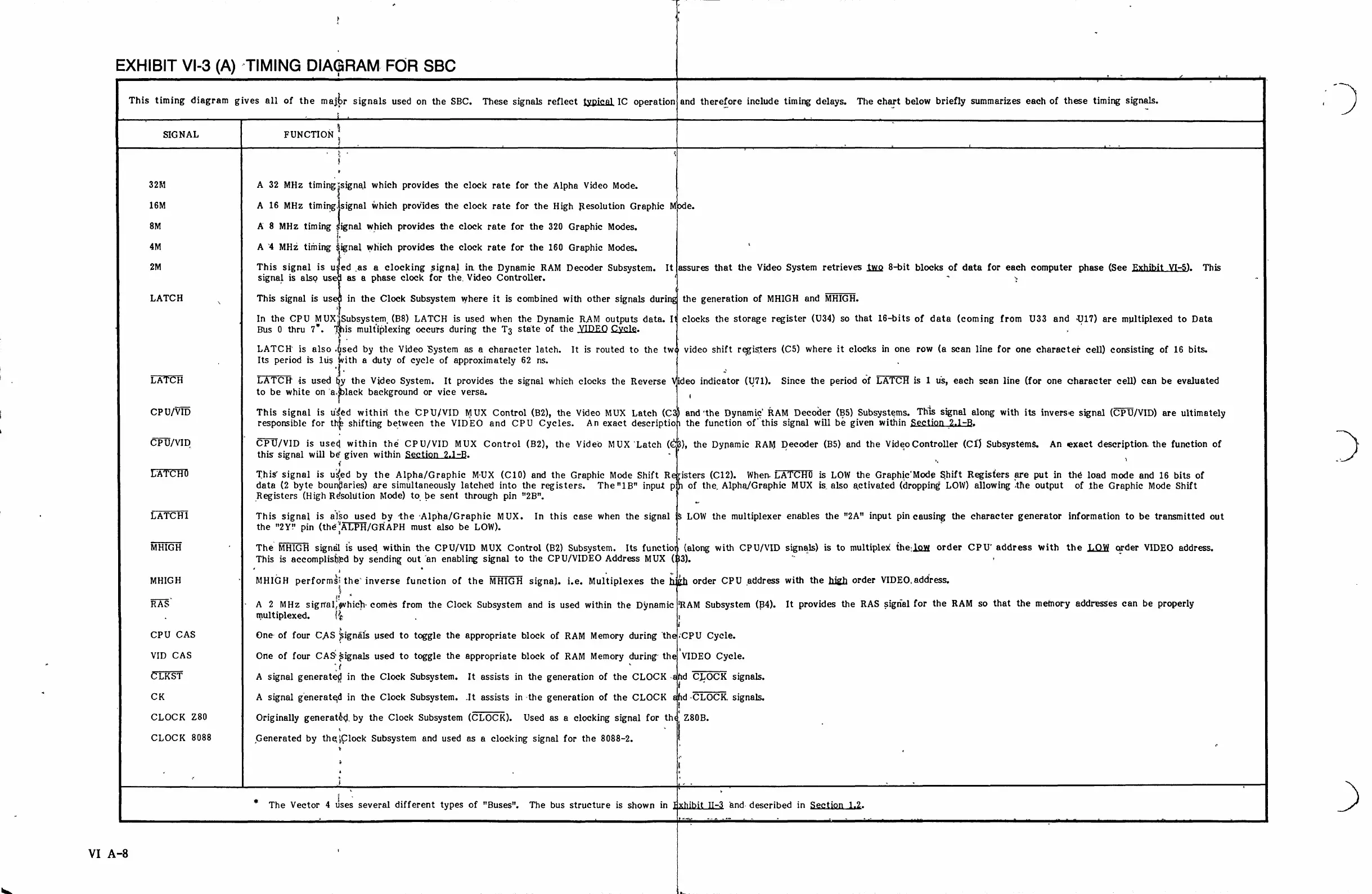
EXHIBIT
VI-3
(A)
“TIMING
DIAGRAM
FOR
SBC
This
timing
diagram
gives
all of
the
maj%r
signals
used
on
the
SBC.
These
signals
reflect
fypical
IC
operation
and
therefore
include
timing
delays.
The
chart
below
briefly
summarizes
each
of
these
timing
signals.
i
SIGNAL
FUNCTION
Z
h
:
L
i
1
32M
A
32
MHz
tlmmg
signal
which
provides
the
clock
rate
for
the
Alpha
Video
Mode.
16M
A
16
MHz
timingjsxgnal
which
provides
the
clock
rate
for
the
High
Resolution
Graphic
Mpde.
8M
A
8
MHz
timing
signal
which
provides
the
clock
rate
for
the
320
Graphic
Modes.
4M
A
‘4
MHz
timing
%gnal
which
provides
the
clock
rate
for
the
160
Graphie
Modes.
'
2M
This
51gnal
is
used
as
a
clocking
signal
in
the
Dynamic
RAM
Decoder
Subsystem.
It{assures
that
the
Video
System
retrieves
fwo
8-bit
blocks
of
data
for
each
computer
phase
(See
Exhibit
VI-§).
This
signal
is
also
usedl
as
a
phase
clock
for
the
Video
Controller.
y
-
¥
LATCH
This
signal
is
us
in
the
Clock
Subsystem
where
it
is
combined
with
other
signals
during
the
generation
of
MHIGH
and
MHIGH.
In
the
CPU
MUX
Subsystem
(B8)
LATCH
is
used
when
the
Dynamic
RAM
outputs
data.
If{
clocks
the
storage
register
(U34)
so
that
16-bits
of
data
(coming
from
U33
and
Ul17)
are
mpultiplexed
to
Data
Bus
0
thru
7.
'I{hls
multiplexing
oceurs
during
the
T3
state
of
the
YIDEOQ
Cycle.
,
LATCH
is
also
rased
by
the
Video
System
as
a
character
latch.
It
is
routed
to
the
tw¢
video
shift
registers
(C5)
where
it
clocks
in
one
row
(a
scan
line
for
one
character
cell)
consisting
of
16
bits.
Its
period
is
1lus
With
a
duty
of
cycle
of
approximately
62
ns.
LATCH
LATCRH
is
used
Qy
the
Video
System.
It
provides
the
signal
which
clocks
the
Reverse
Vfideo
indicator
(U71).
Since
the
period
of
LATCH
is
1
us,
each
scan
line
(for
one
character
cell)
can
be
evaluated
to
be
white
on
a?:lack
background
or
vice
versa.
.
CPU/VID
This
signal
is
uded
withii
the
CPU/VID
MUX
Control
(B2),
the
Video
MUX
Latch
(C3)
and
‘the
Dynamic’
RAM
Decoder
(B5)
Subsystems.
This
signal
along
with
its
inverse
signal
(CPU/VID)
are
ultimately
responsible
for
th“p
shifting
between
the
VIDEO
and
CPU
Cyecles.
An
exact
descriptiop
the
function
of
this
signal
will
be
given
within
Section
2.1-B.
CPU/VID
CPU/VID
is
used
within
the
CPU/VID
MUX
Control
(B2),
the
Video
MUX
‘Latch
(C‘B),
the
Dynamic
RAM
Decoder
(BS)
and
the
Video
Controller
(CI)
Subsystems.
An
exact
description
the
function
of
this
signal
will
be‘
given
within
Section
2.1-B.
!
\
LATCHO
This
signal
is
us’ed
by
the
Alpha/Graphic
M-UX
(C10)
and
the
Graphic
Mode
Shift
Registers
(C12).
When
LATCHO
is
LOW
the
Graphic'Mode
Shift
Registers
are
put
in
thé¢
load
mode
and
16
bits
of
data
(2
byte
bounganes)
are
simultaneously
latched
into
the
registers.
The"1B"
input
pin
of
the
Alpha/Graphic
MUX
is
also
activated
(dropping
LOW)
allowing
the
output
of
the
Graphic
Mode
Shift
Registers
(High
Résolition
Mode)
to
be
sent
through
pin
"2B",
LATCH1
This
sxgnal
is
also
used
by
the
-‘Alpha/Graphic
MUX.
In
this
case
when
the
signal
5§
LOW
the
multiplexer
enables
the
"2A"
input
pin
causing
the
character
generator
information
to
be
transmitted
out
the
"2Y"
pin
(the’
AE
H/GRAPH
must
also
be
LOW).
’
MHIGH
The
MHIGR
signal
is
used
within
the
CPU/VID
MUX
Control
(B2)
Subsystem.
Its
functio
(along
with
CPU/VID
sxgnals)
is
to
multiplex
the:low
order
CPU’
address
with
the
LOW
order
VIDEO
address.
This
is
accomplxshfied
by
sending
out
‘an
enabling
signal
to
the
CPU/VIDEO
Address
MUX
(B3).
)
MHIGH
MHIGH
performs;
the
inverse
function
of
the
MHIGH
signal.
i.e.
Multxplexes
the
h}éh
order
CPU
address
with
the
high
order
VIDEO.
address.
RAS
A
2
MHz
signal,which-
comés
from
the
Clock
Subsystem
and
is
used
within
the
Dynamic
'/RAM
Subsystem
(B4).
It
provides
the
RAS
signal
for
the
RAM
so
that
the
memory
addresses
can
be
properly
multiplexed.
{%
:
i
CPU
CAS
One
of
four
CAS
fsignél’s
used
to
toggle
the
appropriate
block
of
RAM
Memory
during
the:CPU
Cycle.
VID
CAS
One
of
four
CASifsignals
used
to
toggle
the
appropriate
block
of
RAM
Memory
during
the|
VIDEO
Cycle.
R
’
—_—
CLKST
A
signal
generated
in
the
Clock
Subsystem.
It
assists
in
the
generation
of
the
CLOCK
-
?d
CLOCK
signals.
CK
A
signal
generated
in
the
Clock
Subsystem.
.It
assists
in-the
generation
of
the
CLOCK
jhd
-CLOCK
signals.
CLOCK
780
Originally
generatéd
by
the
Clock
Subsystem
(CLOCK).
Used
as
a
clocking
signal
for
thei
Z80B.
CLOCK
8088
Generated
by
thq;Clock
Subsystem
and
used
as
a
clocking
signal
for
the
8088-2.
'
*
&
i
i
<
¥
*
The
Vector
4
l%ses
several
different
types
of
"Buses".
The
bus
structure
is
shown
in
E
+
w
and
described
in
Section
1,2.
o
g
o
o
e
s
- -
o a
_
o
-
oo
i
.
L
P