Do you have a question about the Velleman K8055N and is the answer not in the manual?
Provides general information and links for software and manual translations.
Details the minimum hardware and OS requirements for the device operation.
Lists the technical features and capabilities of the USB experiment interface board.
Offers crucial advice and tips for a successful and safe assembly process.
Explains how to identify resistors and their color codes for proper installation.
Guides the installation of jumpers and emphasizes correct diode polarity.
Details the installation of ceramic capacitors, LEDs (with polarity), and IC sockets.
Covers installation of headers, quartz crystal, and screw connectors.
Provides instructions for installing the LM317 voltage regulator.
Explains how to configure gain settings for analog inputs using resistors.
Details how to connect the board and configure basic settings for operation.
Instructs on selecting the correct address within the test program for device communication.
Explains how to simulate input signals using push buttons for testing.
Details the steps for testing digital outputs by ticking corresponding checkboxes.
Illustrates the electrical connections for analog inputs and PWM outputs.
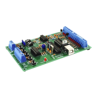
Diagram showing the physical layout of components and connectors on the PCB.
Presents the detailed electronic schematic of the USB experiment interface board.
| Category | Computer Hardware |
|---|---|
| Interface | USB |
| Digital Inputs | 5 |
| Analog Inputs | 2 |
| Analog Outputs | 2 |
| Power Supply | USB powered |
| Analog Output Resolution | 8 bit |
| Analog Input Resolution | 8 bit |
| Analog Output | 0-5V |
| Operating System Compatibility | Windows |
| Type | USB Experiment Interface Board |
| Digital Outputs | 8 (open collector, max. 50V/100mA) |
| Counter Inputs | 2 |