SECTION
4
CIRCUIT DESCRIPTION
4.1 FUNCTION GENERATOR
As
shown
in figure 4-1,
the
VCG summing
amplifier sums
the
currents from the frequency dial and VCG
input
con-
nector in function generator mode or from
the low
pass
filter
output and the.frequency-to-voltage
(F/V)
converter
output in synthesizer mode. The low pass
filter
is part of
the generator frequency phase lock loop
which
provides a
feedback current that
corrects generator
frequency to
be
exactly that of
the synthesizer loop output.
(Phase lock
loop operation is described in paragraph
4.5.)
The
F/V
input
is also from the
synthesizer
loop and
provides a gross
cor-
rection
to
increase the response time of the
generator to
changes in synthesizer frequency programming.
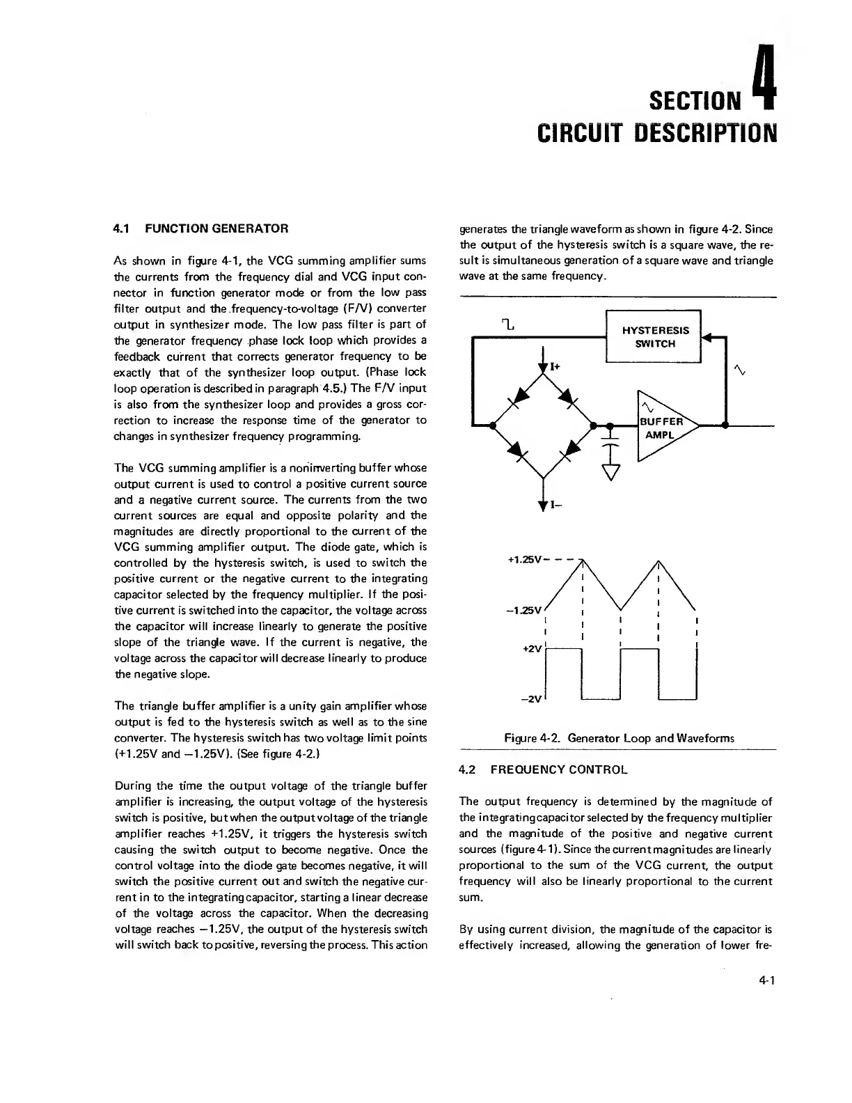
The VCG summing amplifier is
a
noninverting buffer
whose
output current is used
to
control
a
positive
current source
and
a
negative
current
source.
The currents from the two
current sources are equal and
opposite polarity and
the
magnitudes are directly proportional
to
the
current of the
VCG
summing amplifier output. The diode gate,
which is
controlled
by the hysteresis switch, is used to
switch
the
positive current or the
negative current
to the
integrating
capacitor selected
by
the
frequency multiplier. If the
posi-
tive current is switched into the capacitor, the voltage across
the
capacitor will increase linearly to generate the positive
slope of
the
triangle wave. If
the
current is negative, the
voltage across the capacitor will decrease linearly
to
produce
the negative slope.
The triangle buffer amplifier is
a
unity gain
amplifier
whose
output is fed
to
the hysteresis
switch as
well
as to
the
sine
converter. The hysteresis switch has
two
voltage limit points
(+1.25V and
-1.25V).
(See figure
4-2.)
During the time the output voltage of
the
triangle
buffer
amplifier is
increasing, the output voltage of the
hysteresis
switch is
positive,
but
when
the
output
voltage
of
the
triangle
amplifier reaches
+1.25V, it triggers the hysteresis switch
causing the switch output
to become negative. Once the
control
voltage
into the diode gate becomes negative, it will
switch the positive current out and switch
the
negative cur-
rent in to
the
integrating
capacitor, starting
a
linear decrease
of the voltage across the capacitor. When
the
decreasing
voltage reaches —1.25V, the output of
the hysteresis switch
will
switch back
to
positive, reversing the
process. This action
generates the triangle waveform as shown
in figure
4-2.
Since
the
output of the
hysteresis
switch is
a
square
wave, the
re-
sult is simultaneous generation
of a square wave and triangle
wave
at
the same frequency.
Figure
4-2.
Generator
Loop and
Waveforms
4.2 FREQUENCY CONTROL
The
output
frequency
is determined
by the magnitude of
the integratingcapacitor
selected
by the frequency multiplier
and the magnitude of the
positive and
negative
current
sources (figure
4-1).
Since thecurrentmagnitudes
are
linearly
proportional
to
the sum of
the VCG current, the output
frequency will
also be
linearly
proportional to the current
sum.
By using current division, the magnitude of the capacitor is
effectively
increased,
allowing
the generation of lower
fre-
4-1
 Loading...