EasyManua.ls Logo

Winbond Spiflash W25Q80BV User Manual

Winbond Spiflash W25Q80BV
80 pages
To Next Page IconTo Next Page
Page #1 background imageLoading...
Page #1 background image
W25Q80BV
Publication Release Date: Augest 01, 2012
- 1 - Revision G
8M-BIT
SERIAL FLASH MEMORY WITH
DUAL AND QUAD SPI

Table of Contents

Question and Answer IconNeed help?

Do you have a question about the Winbond Spiflash W25Q80BV and is the answer not in the manual?

Winbond Spiflash W25Q80BV Specifications

General IconGeneral
Memory Density8 Mbit
Memory Size1 MB
InterfaceSPI
Clock Frequency104 MHz
Operating Temperature-40°C to +85°C
Package TypeSOIC
Data Retention20 years
Memory TypeNOR Flash
Voltage Range2.7V - 3.6V
Package / Case8-SOIC

Summary

General Description

Features

High Performance Serial Flash

Details high performance specifications for the serial flash memory.

Advanced Security Features

Outlines the security features like write protection and unique serial numbers.

Space Efficient Packaging

Lists the available compact package types for the device.

Package Types and Pin Configurations

Pin Configuration SOIC / VSOP 150 / 208-mil

Shows pin assignments for SOIC and VSOP packages.

Pad Configuration WSON 6x5-mm / USON 2x3-mm

Shows pad assignments for WSON and USON packages.

Pin Description SOIC, VSOP, WSON & PDIP 300-mil

Pin Descriptions

Chip Select (/CS)

Explains the function and operation of the Chip Select pin.

Serial Data Input, Output and IOs (DI, DO and IO0, IO1, IO2, IO3)

Describes the serial data pins and their use in different SPI modes.

Block Diagram

Functional Description

SPI Operations

Details SPI operation modes, including Dual and Quad SPI.

Write Protection

Control and Status Registers

Status Register

Explains the status register and its various bits.

Status Register Protect (SRP1, SRP0)

Security Register Lock Bits (LB3, LB2, LB1)

Quad Enable (QE)

Status Register Memory Protection (CMP = 0)

Instructions

Manufacturer and Device Identification

Details how to identify the manufacturer and device.

Instruction Set Table 1 (Erase, Program)

Instruction Set Table 2 (Read)

Write Enable (06h)

Write Status Register (01h)

Read Data (03h)

Fast Read (0Bh)

Fast Read Quad Output (6Bh)

Fast Read Dual I/O (BBh)

Fast Read Quad I/O (EBh)

Word Read Quad I/O (E7h)

Octal Word Read Quad I/O (E3h)

Page Program (02h)

Sector Erase (20h)

32KB Block Erase (52h)

64KB Block Erase (D8h)

Chip Erase (C7h / 60h)

Erase / Program Suspend (75h)

Power-down (B9h)

Release Power-down / Device ID (ABh)

Read Manufacturer / Device ID (90h)

Read Manufacturer / Device ID Quad I/O (94h)

Read Unique ID Number (4Bh)

Read JEDEC ID (9Fh)

Read SFDP Register (5Ah)

Erase Security Registers (44h)

Program Security Registers (42h)

Electrical Characteristics

Absolute Maximum Ratings

Lists the absolute maximum electrical ratings for the device.

Operating Ranges

Specifies the recommended operating voltage and temperature ranges.

DC Electrical Characteristics

AC Electrical Characteristics

Serial Output Timing

Serial Input Timing

Package Specification

8-Pin SOIC 150-mil (Package Code SN)

Details the dimensions and specifications for the 8-Pin SOIC 150-mil package.

8-Pad WSON 6x5mm (Package Code ZP)

8-Pad USON 2x3-mm (Package Code UX)

Ordering Information

Valid Part Numbers and Top Side Marking

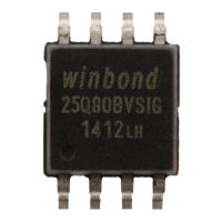
Lists valid part numbers and their corresponding top side markings.

Revision History