292 Chapter6
Troubleshooting the RF Section
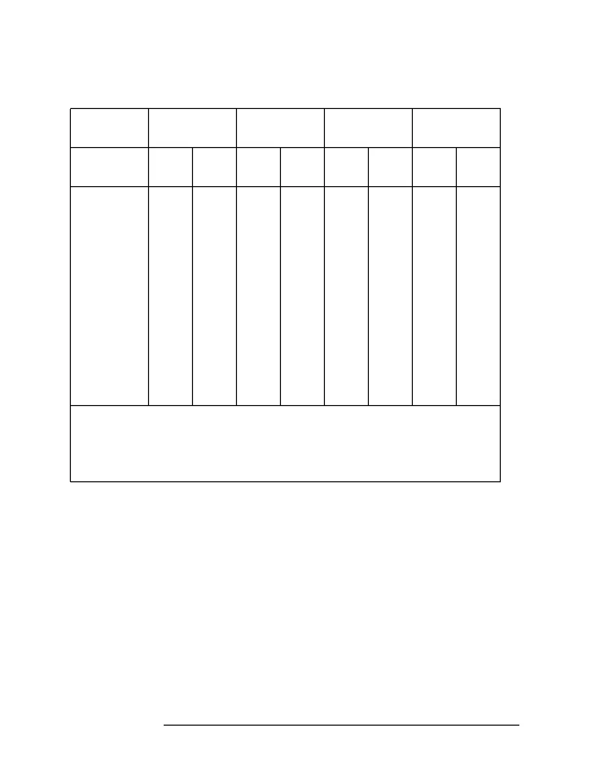
6b. 8592L/94L, 8594Q, and 8593E/94E/95E/96E
Table 6-11 Input Attenuator Control Output at A7J5 for 8594E,
8594L, 8594Q, 8595E, 8596E
10 dB 40 dB 20 dB Blocking
Step Step Step Capacitor
Attenuator
Setting (dB) Pin 2 Pin 1 Pin 9 Pin 4 Pin 8 Pin 5 Pin 7 Pin 6
0 HLHLHL——
10 LHHLHL——
20 HLHLLH——
30 LHHLLH——
40 HLLHHL——
50 LHLHHL——
60 HLLHLH——
70 LHLHLH——
Blocking
Capacitor In
—————— L H
Blocking
Capacitor Out
——————H L
H = −10 V (with the attenuator connected at A7J5)
H = 0 V (A floating output if the attenuator is disconnected.)
L = −15 V (A low at pin 2, 9, or 8 indicates that the attenuator step is in
the signal path. A low at pin 7 indicates the blocking capacitor is the signal path.)
 Loading...