EasyManua.ls Logo

Ai-Thinker Technology ESP-12F - User Manual

Ai-Thinker Technology ESP-12F
17 pages
Print Icon
To Next Page IconTo Next Page
Loading...
ESP-12F User Manual
REV:2.0
2017.8
Question and Answer IconNeed help?

Do you have a question about the Ai-Thinker Technology ESP-12F and is the answer not in the manual?

Summary

1. Preambles

1.1. Features

Lists the key features of the ESP-12F module, including Wi-Fi standards, MCU, ADC, and protocol stack.

1.2. Parameters

Details major parameters like Wi-Fi protocols, frequency range, and hardware/software specifications.

2. Pin Descriptions

2.1. Interfaces

Describes various interfaces like HSPI, PWM, IR Remote Control, ADC, I2C, UART, and I2S.

2.2. Pin Mode

Outlines the pin modes for GPIO15, GPIO0, and GPIO2 during UART and Flash Boot operations.

2.3. Antenna interface

Specifies requirements for connecting external antennas to the ESP-12F module.

3. Package information and OEM installation method

3.1. Package information

Provides dimensions and PCB footprint details for the ESP-12F WiFi module.

3.2. OEM installation method

Guides on module installation, layout, and reflow soldering temperature curves for OEM.

4. Absolute Maximum Ratings

4.1. Recommended Operating Conditions

Details the recommended operating temperature and supply voltage for the ESP-12F module.

4.2. AT commend Testing

Explains hardware connection and software tools for testing the ESP-12F module using AT commands.

4.3. AT commend

Covers the AT command set, including command types and basic command descriptions.

Overview

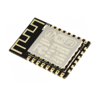
The ESP-12F WiFi module, developed by Ai-Thinker Co., Ltd, is a compact and highly integrated wireless SOC designed for mobile platform designers with space and power constraints. It leverages the ESP8266 core processor, which features a Tensilica L106 Diamond series 32-bit MCU. This module offers an unsurpassed ability to embed Wi-Fi capabilities into other systems or to function as a standalone application, providing a cost-effective and minimal space solution.

Function Description

The ESP-12F module provides a complete and self-contained Wi-Fi networking solution. It can either host the application directly or offload Wi-Fi networking functions to another application processor. When hosting an application, it boots directly from an external flash and includes integrated cache for improved performance. Alternatively, it can serve as a Wi-Fi adapter, adding wireless internet access to any microcontroller-based design via simple connectivity interfaces such as SPI/SDIO or I2C/UART.

The module supports the standard IEEE802.11 b/g/n agreement and a complete TCP/IP protocol stack, allowing users to integrate it into existing device networks or build separate network controllers. It also integrates antenna switches, an RF balun, a power amplifier, a low-noise receive amplifier, filters, and power management modules, requiring minimal external circuitry. The entire solution, including the front-end module, is designed to occupy minimal PCB area.

The ESP8266EX processor includes on-chip SRAM and Wi-Fi functionalities. It can be integrated with external sensors and other application-specific devices through its GPIOs, with example codes provided in the SDK. The module supports various operation modes, including STA, AP, and STA+AP, and features Smart Link Functionality for both Android and iOS devices.

Important Technical Specifications

General Parameters:

  • Operating Voltage: 3.3V
  • Operating Current: Average value: 80mA
  • Operating Temperature Range: -40°C to 125°C
  • Ambient Temperature Range: Normal temperature
  • Package Size: 18mm x 20mm x 3mm
  • External Interface: N/A
  • Wi-Fi Mode: Station/SoftAP/SoftAP+Station
  • Security: WPA/WPA2
  • Encryption: WEP/TKIP/AES
  • Network Protocols: IPv4, TCP/UDP/HTTP/FTP
  • User Configuration: AT Instruction Set, Cloud Server, Android/iOS APP

Wi-Fi Parameters:

  • Wi-Fi Protocols: 802.11 b/g/n
  • Frequency Range: 2.4GHz-2.5GHz (2400M-2483.5M)
  • Output Power: +20dBm in 802.11b mode
  • Antenna: Supports antenna diversity, connects to external antenna via IPEX interface.
    • Antenna Frequency Range: 2.4~2.4825GHz
    • Antenna Impedance: 50Ω

Hardware Parameters:

  • MCU: Integrated low power 32-bit MCU (Tensilica L106 Diamond series)
  • Clock Speed: Supports 80 MHz, 160 MHz
  • ADC: Integrated 10-bit ADC (input voltage range 0~1V, value range: 0~1024)
  • Peripheral Bus: UART/HSPI/I2C/I2S/Ir Remote Control, GPIO/PWM
  • Integrated Components: TR switch, balun, LNA, power amplifier, matching network, PLL, regulators, power management units.
  • MIMO: STBC, 1x1 MIMO, 2x1 MIMO
  • Aggregation: A-MPDU & A-MSDU aggregation and 0.4s guard interval

Power Consumption:

  • Deep Sleep Power: <10uA
  • Power Down Leakage Current: < 5uA
  • Wake Up and Transmit: < 2ms
  • Standby Power Consumption (DTIM3): < 1.0mW

Pin Descriptions (16 pins):

  • RST (Pin 1): Reset module
  • ADC (Pin 2): A/D conversion result (0-1V input, 0-1024 value)
  • EN (Pin 3): Chip enable pin, active high
  • GPIO16 (Pin 4): Can wake up chipset from deep sleep mode
  • GPIO14 (Pin 5): HSPI_CLK
  • GPIO12 (Pin 6): HSPI_MISO
  • GPIO13 (Pin 7): HSPI_MOSI; UARTO_CTS
  • VCC (Pin 8): 3.3V power supply (VDD)
  • CS0 (Pin 9): SPI CS0; GPIO11
  • MISO (Pin 10): SPI MISO; GPIO7
  • GPIO9 (Pin 11): SPI HD; GPIO9
  • GPIO10 (Pin 12): SPI WP; GPIO10
  • MOSI (Pin 13): SPI MOSI; GPIO8
  • CLK (Pin 14): SPI CLK; GPIO6
  • GND (Pin 15): Ground
  • GPIO15 (Pin 16): MTDO; HSPICS; UARTO_RTS
  • GPIO2 (Pin 17): UART1_TXD
  • GPIO0 (Pin 18): GPIO0
  • GPIO4 (Pin 19): GPIO4
  • GPIO5 (Pin 20): GPIO5
  • RXD0 (Pin 21): UARTO_RXD; GPIO3
  • TXD0 (Pin 22): UARTO_TXD; GPIO1

Pin Mode for UART and Flash Boot:

Mode GPIO15 GPIO0 GPIO2
UART low low high
Flash Boot low high high

Usage Features

Firmware Upgrade:

  • Supports UART Download / OTA (via network)
  • Download and write firmware via host

Software Development:

  • Supports Cloud Server Development
  • SDK for custom firmware development

Interfaces:

  • HSPI: Connects SPI Flash, display screens, and MCUs.
  • PWM: Four channels, extendable by users, used to control LED lights, buzzers, relays, and electronic machines.
  • IR Remote Control: Implemented via software programming, uses NEC coding, modulation, and demodulation with a 38KHz modulated carrier signal.
  • ADC: Used to test power supply voltage (VDD3P3) and input power voltage (TOUT). These two functions cannot be used simultaneously.
  • I2C: Connects external sensor products and display screens.
  • UART:
    • Downloading: U0TXD+U0RXD or GPIO2+U0RXD
    • Communicating: UARTO: UOTXD, UORXD, MTDO (UORTS), MTCK (UOCTS)
    • Debugging: UART1_TXD (GPIO2) for printing debug information.
    • UARTO outputs printed information during power-on and boot-up. Users can exchange inner UART pins (UOTXD, UORXD with UORTS, UOCTS) if this affects specific applications.
  • I2S: Mainly used for collecting, processing, and transmitting audio data.

AT Command Set: The module can be driven via the serial interface using standard AT commands, which are divided into Basic AT commands, Wi-Fi related AT commands, and TCP/IP AT commands.

  • AT+=?: Test command, queries internal parameters and their range values.
  • AT+?: Query command, returns the current value of a parameter.
  • AT+=<...>: Set command, sets user-defined parameters.
  • AT+: Execute command, runs commands with no user-defined parameters.

Basic AT Commands:

  • AT: Test AT startup (returns OK).
  • AT+RST: Restart module (returns OK).
  • AT+GMR: View version info (AT version, SDK version, compile time).
  • AT+GSLP= Enter deep-sleep mode for a specified time (in ms). Requires connecting XPD_DCDC with EXT_RSTB via OR.
  • ATE0/ATE1: Control AT commands echo (0 for off, 1 for on).
  • AT+RESTORE: Factory reset, restores default settings and restarts the chip.
  • AT+UART / AT+UART_CUR / AT+UART_DEF: UART configuration.
  • AT+SLEEP: Sleep mode.
  • AT+RFPOWER: Set maximum RF TX Power.
  • AT+RFVDD: Set RF TX Power according to VDD33.

Maintenance Features

OEM Installation Method: The ESP-12F module uses a half-hole patch package. For OEM installation, it is crucial to reference the package information and layout on the main board. The module's direction and antenna placement are important; the antenna should be close to the edge of the board, and components/layout should not be directly beneath the antenna.

Soldering Recommendations:

  • Maximum Soldering Temperature: 260°C
  • Reflow Soldering Temperature Curves: Adhere to IPC/JEDEC standard.
    • Peak Temperature: <250°C (≤2 times)
    • Preheat: 150-200°C for 60-120 seconds
    • Ramp-up Rate: Max. 2°C/sec
    • Ramp-down Rate: Max. 2.5°C/sec
    • Time above 217°C: 40-60 seconds
    • Soldering should not be performed in high-temperature environments.

Module Limitations:

  • The module is limited to OEM installation ONLY.
  • The OEM integrator is responsible for ensuring the end-user has no manual instruction to remove or install the module.
  • The module is limited to installation in mobile applications.
  • A separate approval is required for all other operating configurations, including portable configurations (Part 2.1093) and different antenna configurations.
  • The grantee must provide guidance to the host manufacturer for compliance with Part 15B requirements.

Ai-Thinker Technology ESP-12F Specifications

General IconGeneral
BrandAi-Thinker Technology
ModelESP-12F
CategoryWireless Router
LanguageEnglish