EasyManua.ls Logo

Akai AM-M630 User Manual

Akai AM-M630
60 pages
To Next Page IconTo Next Page
Page #1 background imageLoading...
Page #1 background image
Question and Answer IconNeed help?

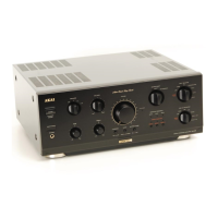
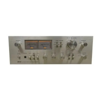
Do you have a question about the Akai AM-M630 and is the answer not in the manual?

Akai AM-M630 Specifications

General IconGeneral
Power Output60 watts per channel into 8Ω (stereo)
Frequency Response5Hz to 100kHz
Total Harmonic Distortion0.05%
Input Sensitivity2.5mV (MM), 150mV (line)
Dimensions425 x 148 x 350mm
Weight9.5kg
Signal to noise ratio80dB (MM), 95dB (line)
Speaker Impedance4Ω to 16Ω
Damping factor60 (8 ohms)
Channel separation60dB (1kHz)

Summary

Specifications

Safety Instructions and Precautions

Servicing Safety Precautions

Guidelines for safe and compliant servicing procedures, including critical part replacement.

Recommended Spare Parts

Control PCB Schematic Details

Control PCB Signal Path Diagram

Illustrates signal flow and component connections on the Control PCB.

Control and Power PCB Schematics

Overall System Block Diagram

Interconnected Functional Blocks

High-level diagram showing interconnections between major PCBs like Control, VR, Power, and Main Amp.

VR and Phone PCB Schematics

DAC-A PCB Schematic Details

DAC-A PCB Circuit and Pinout Information

Detailed schematic of the DAC-A PCB, including IC pinouts and signal lines.

DAC-A PCB Schematic - Circuit Analysis

DAC-A PCB Component Connections and Voltages

Schematic showing component connections and measured voltages on the DAC-A PCB.

DAC-A PCB Schematic - Signal and Power

DAC-B PCB Schematic Details

DAC-B PCB Layout and Component Identification

Schematic diagram and principal parts location for the DAC-B PCB.

DAC-B PCB Schematic - Circuit Analysis

DAC-B PCB Component Connections and Voltages

Detailed schematic for DAC-B PCB, showing ICs, transistors, and voltage levels.

DAC-B PCB Schematic - Signal and Power

DAC-B PCB Schematic - Further Details

PCB Connection Diagrams

JACK PCB Interconnection Diagram

Shows connections between the JACK PCB and other system components.

PHONE PCB Interconnection Diagram

Illustrates connections for the PHONE PCB to other system parts.

PCB Interconnection Schematics

Main Amplifier PCB Connection Details

Diagram showing how the MAIN AMP PCB connects to DAC-A, DAC-B, and JACK PCBs.

Control and VR PCB Schematics

Filter and LED PCB Schematics

PCB Connection Diagrams - Part 2

Main Amplifier PCB Connection Details

Main AMP PCB Interfacing with Other PCBs

Details connections of the MAIN AMP PCB to various other PCBs and power sources.

Filter, Control, and VR PCB Schematics

System Connection Schematics

Filter PCB AC Power Input and Selection

Diagram of Filter PCB showing AC power input and voltage selection.

Control PCB System Power and Signal Distribution

Schematic illustrating Control PCB's role in system power and signal distribution.

Main Amplifier PCB Schematic - Part 1

Main Amp PCB Signal Path Diagram

Schematic detailing signal flow and component locations on the Main Amplifier PCB.

Main Amplifier PCB Schematic - Part 2

Main Amp PCB Power Lines and Connections

Schematic showing power supply lines and component interconnections on the Main AMP PCB.

Main Amplifier PCB Schematic - Part 3

Main Amp PCB IC and Transistor Schematics

Detailed schematics of ICs and transistors on the Main Amplifier PCB.

Main Amplifier PCB Schematic - Part 4

Main Amplifier PCB Schematic - Part 5

Main Amp PCB Fuse and Power Circuitry

Details fuse circuits and power supply components on the Main Amplifier PCB.

Main Amplifier PCB Schematic - Part 6

Main Amp PCB Transistor and Diode Schematics

Schematic details for transistors and diodes on the Main Amplifier PCB.

Main Amplifier PCB Schematic - Part 7

Main Amp PCB IC and Connector Schematics

Focuses on ICs and connector pinouts on the Main Amplifier PCB.

Main Amplifier PCB Schematic - Part 8

Main Amp PCB IC and Transistor Circuit Details

Final schematic details for transistors and ICs on the Main Amplifier PCB.

Control PCB Schematic - Part 1

Control PCB Schematic - Part 2

Control PCB Schematic - Part 3

Control PCB Schematic - Part 4

LED (L) PCB Schematic Details

LED (R) PCB Schematic Details

Control PCB Schematic - Part 5

Control PCB Schematic - Part 6

Related product manuals