Alesis D4/D5 Drum Modules Service Manual 5 02/19/03
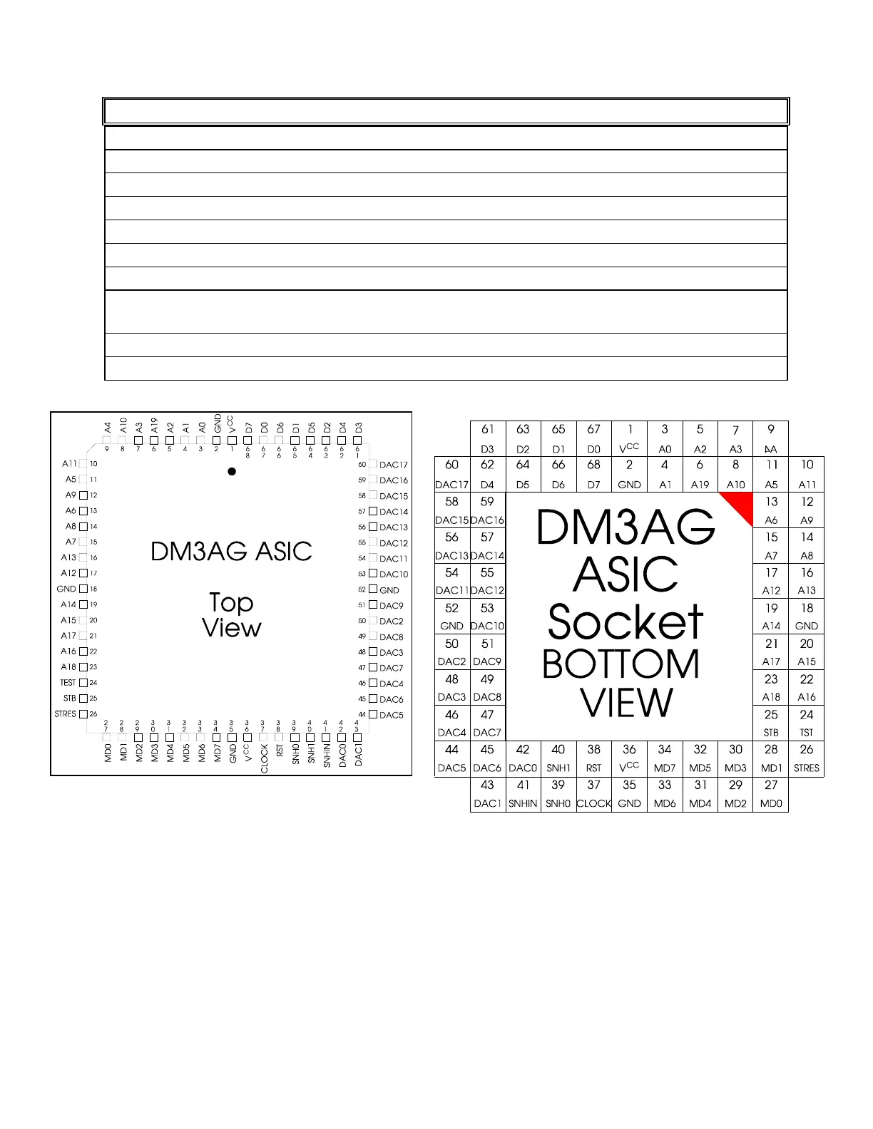
NAME PIN#(s) Function
MD0-MD7 27-34 8031 Data Buss Input.
CLOCK 37 Asic Clock Input (8MHz in SR-16).
DAC0-DAC16 42-51, 53-60 Output to DAC.
A0-A19 3-17, 19-23 Mask Address Buss
D0-D7 61-68 Mask Rom Data Buss
SNH0 39 Output Sample and Hold Control
SNH1 40 " " " " "
SNHIN 41 Output Sample and Hold
Inhibit.
STRES 26 Instruction reset strobe.
STB 25 Instruction latch strobe.
3.21 Address Buss Decoding
Due to the fact that we are pushing the ASIC beyond it's original design, a little extra hardware
was required to accomplish the design goals of the D4. Two limitations needed to overcome. 1> The
address space directly accessible wasn't enough for all of the samples. 2> The ASIC clock speed was
increased from earlier designs to 12MHz, making extra communication from the 8031 more difficult.
This solution to these problems takes the form of an asynchronous decoder. The purpose of the
decoder is to act as an extra set of address lines to ensure that only one Mask ROM is enabled at any
given time.
Diagram 5
Diagram 2


 To Next Page