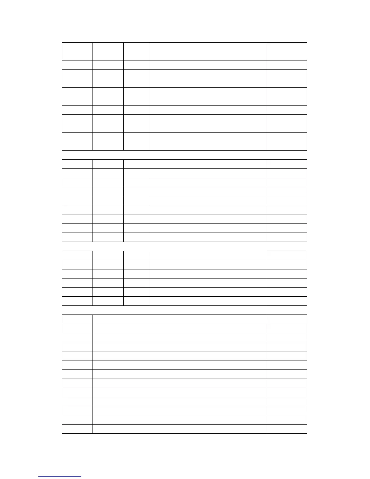
58 TMS D In JTAG Test Mode Select with internal
pullup
3.25
59 TCK D In JTAG Test Clock with internal pullup 3.28
60 TDI D In JTAG Test Data output with internal
pullup
3.25
61 TDO D Out JTAG Test Data Output with internal
pull up
3.25
62 /RST D I/O Device Reset 3.21
63 DAC1 A Out Digital to Analog Converter 1 Voltage
Output
0.13
64 DAC0 A Out Digital to Analog Converter 0 Voltage
Output
0.13
EEPROM 24C02 (U19)
Pin No. Name Type Function Voltage(V)
1 A0 In Address inputs 0.04
2 A1 In Address inputs 0.04
3 A2 In Address inputs 0.04
4 VSS Gnd Negativ power supply 0
5 SDA I/O Serial data input/output 4.01
6 SCL I Serial clock data input 4.01
7 WP In Write Protect 0.04
8 VCC PI Positive power supply 5.38
DC-DC Converter AP1506 (U20)
Pin No. Name Type Function Description Voltage(V)
1 Vin PI Operating voltage input 11.07
2 Output Out Switching output 4.16
3 GND Gnd Ground 0
4 FB In Output voltage feedback control 1.22
5 SD In /ON/OFF Shutdown 0.06/4.95
Dual preamplifier with ALC BA3308F(U21)
Pin No. Function Voltage(V)
1 OUTPUT1 1.96
2 GND 0
3 NC 0.23
4 ALC 1.28
5 VCC 7.19
6 NC 0.24
7 OUTPUT2 1.97
8 NC 0.24
9 INPUT2 0.05
10 NF2 1.96
11 NF1 1.95
12 NC 0.24
ˋ