AD9854
Rev. E | Page 39 of 52
SDIO
D
7
I
7
CLK
INSTRUCTION CYCLE
D
T
TRANSFER CYCLE
I
6
I
5
I
4
I
3
I
0
I
2
I
1
D
6
D
5
D
4
D
3
D
2
D
1
D
0
CS
00636-058
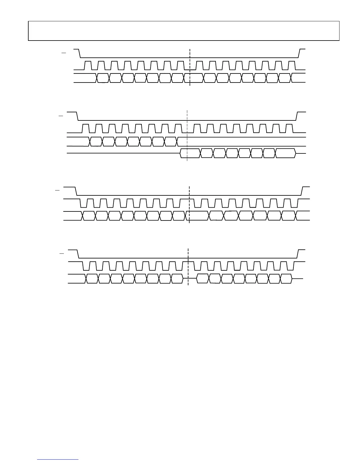
Figure 58. Serial Port Write Timing Clock Stall Low
SDIO
D
O7
D
O6
D
O5
D
O4
D
O3
D
O2
D
O1
D
O0
CLK
INSTRUCTION CYCLE
DON'T CARE
SDO
DATA TRANSFER CYCLE
I
7
I
6
I
5
I
4
I
3
I
0
I
2
I
1
CS
0636-059
Figure 59. 3-Wire Serial Port Read Timing Clock Stall Low
D
7
D
6
D
5
D
4
D
3
D
2
D
1
D
0
SDIO
SCLK
INSTRUCTION CYCLE D
T
TRANSFER CYCLE
I
7
I
6
I
5
I
4
I
3
I
0
I
2
I
1
CS
00636-060
Figure 60. Serial Port Write Timing Clock Stall High
I
7
I
6
I
5
I
4
I
3
I
0
I
2
I
1
SDIO
CL
INSTRUCTION CYCLE D
T
TRANSFER CYCLE
D
O7
D
O6
D
O5
D
O4
D
O3
D
O2
D
O1
D
O0
CS
00636-061
Figure 61. 2-Wire Serial Port Read Timing Clock Stall High
CR [8] is the internal update active bit. When this bit is set to
Logic 1, the I/O UD CLK pin is an output and the AD9854
generates the I/O UD CLK signal. When this bit is set to Logic 0,
external I/O UD CLK functionality is performed and the I/O
UD CLK pin is configured as an input.
CR [7] is reserved. Write to 0.
CR [6] is the inverse sinc filter bypass bit. When this bit is set,
the data from the DDS block goes directly to the output shaped
keying logic, and the clock to the inverse sinc filter is stopped.
Default is clear with the filter enabled.
CR [5] is the shaped keying enable bit. When this bit is set, the
output ramping function is enabled and is performed in
accordance with the CR [4] bit requirements.
CR [4] is the internal/external output shaped keying control bit.
When this bit is set to Logic 1, the output shaped keying factor is
internally generated and applied to both the I and Q paths.
When this bit is cleared (default), the output shaped keying
function is externally controlled by the user, and the ouput
shaped keying factor is the value of the I and Q output shaped
keying factor register. The two registers that are the output
shaped keying factors also default low such that the output is off
at power-up until the device is programmed by the user.
CR [3:2] are reserved. Write to 0.
CR [1] is the serial port MSB-/LSB-first bit. Default is low,
MSB first.
CR [0] is the serial port SDO active bit. Default is low, inactive.
 Loading...