AN-583 Application Note
Rev. D | Page 4 of 4
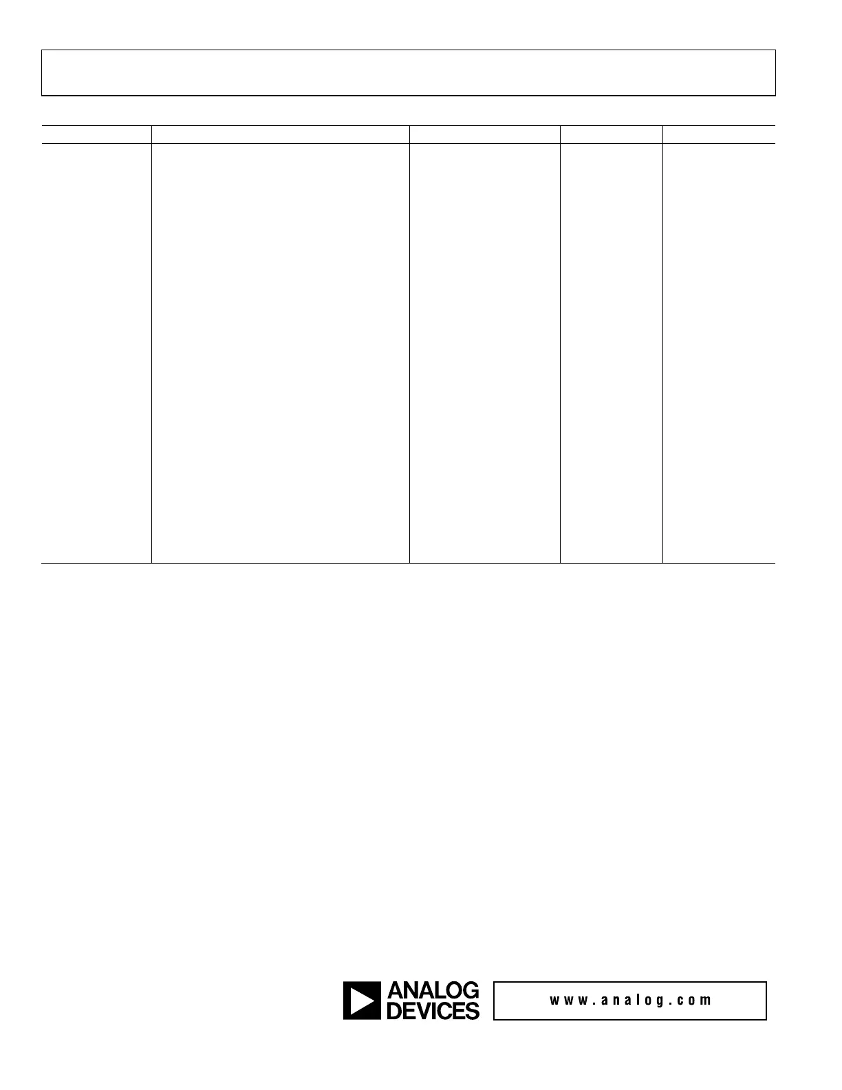
Table 1. Parts List for SSM2167 Evaluation Board
Reference Description Part Number Value Tolerance (%)
U1 Low voltage microphone pre-amp SSM2167-1RMZ SSM2167-1RMZ Not applicable
C1, C10 Chip capacitors, X7R, 0805 GRM21BR71H104KA01L 0.1 µF 10
C2, C3, C9 Tantalum capacitors TAJA106K010RNJ 10 µF 10
C4 Capacitor, ceramic monolithic, X5R GRM31CR61E106KA12L 10 µF 10
C11 Capacitor, ceramic, C0G GRM2165C1H102JA01D Do not install 5
C5 to C8 Capacitors, ceramic, X7R GRM21BR71A106ME51 Do not install 20
J1, J2 3.5 mm stereo jacks SJ1-3525NG SJ1-3525NG Not applicable
JP4, JP5 Headers 10-89-7102 10-89-7102 Not applicable
JP4, JP5 Shunt connector SNT-100-BK-G SNT-100-BK-G Not applicable
JP1, JP2 Headers SSW-102-01-G-S Do not install Not applicable
R10 Resistor, precision thick film chip, R0805 ERJ-6ENF7502V 75 kΩ 1
R11 Resistor film, SMD, 0805 MC 0.1W 0805 1% 15K. 15 kΩ 1
R13 Resistor chip, 0805 MC0805S8F3001T5E 3 kΩ 1
R14 Resistor, precision thick film chip, R0805 ERJ-6ENF2001V 2 kΩ 1
R15 Resistor, precision thick film chip, R0805 ERJ-6ENF1001V 1 kΩ 1
Resistors, thick film chip
R4 Resistor film, SMD, 0805 MC 0.1W 0805 1% 2K2. 2.2 kΩ 1
R5 Resistor, high precision thick film chip PHT0805Y5003BGT200 500 kΩ 0.1
R7 Resistor, precision thick film chip, R0805 ERJ-6ENF1003V 100 kΩ 1
R8 Resistor, precision thick film chip, R0805 ERJ-6ENF1002V 10 kΩ 1
Resistor, precision thick film chip
+3V Test point TP-104-01-02 RED Not applicable
SD Test point TP104-01-06 BLU Not applicable
GND Test point TP-104-01-00 BLK Not applicable
INPUT, OUTPUT Test point TP104-01-08 GRY Not applicable
REVISION HISTORY
10/15—Rev. C to Rev. D
Changes to Title, Shutdown Connection Section, and Signal
Connections, Input, and Output Section ...................................... 1
Changes to Figure 2 .......................................................................... 2
Changes to Figure 3, Figure 4, and Figure 5.................................. 3
Changes to Table 1 ............................................................................ 4
2/13—Rev. B to Rev. C
Changes to Figure 5 .......................................................................... 3
Changes to Table 1 ............................................................................ 4
©2002–2015 Analog Devices, Inc. All rights reserved. Trademarks and
registered trademarks are the property of their respective owners.
AN02728-0-10/15(D)

 Loading...


