S19 Maintenance Guide
11
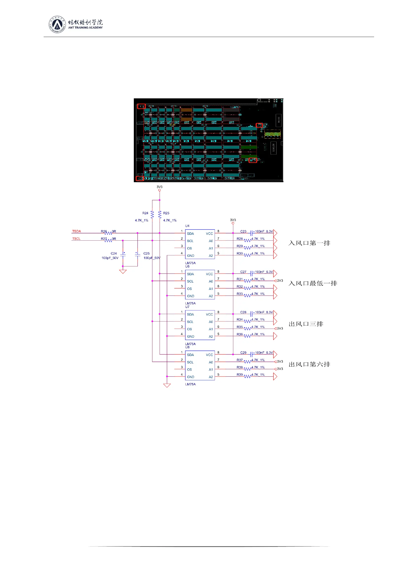
B) Check whether the four temperature senses U4, R28~R30, U6, R31~R33, U7, R34~R36, U8, R37~R39 and the matching resistance
welding are abnormal, the location of the temperature sense is shown in Figure 5-14, the temperature sense is all located on the back of the
PCB, the resistance is located on the front of the PCB, and whether the temperature-sensitive 3.3V power supply is normal;
Check the welding quality of the heat-sensitive chip and the small heat sink. The deformation of the large heat sink material will cause
poor heat dissipation of the chip and affect the temperature difference.
Figure 5-14
4. Phenomenon: Single board detection chip is not complete (PT1/PT2 stations)
a) LCD display ASICNG: if (0), first measure the total voltage of the measuring domain and the boost circuit 19V is normal, and then use
the short-circuit probe to short-circuit the RO test point and the 1V8 test point between the first and the second chip, and then operate the
program to find the chip. Looking at the serial port log, if 0 chip is still found at this time, it will be one of the following situations:
a-1) Use a multimeter to measure whether the voltages at the 1V8 and 0V8 test points are 1.8V or 0.8V. If not, it indicates that the 1.8V or
0.8V LDO circuit of this domain is abnormal, or the two ASIC chips of this domain is not soldered well; most of this are caused by short
circuits of 0.8V, 1.8V patch filter capacitors (measure the resistance of the patch filter capacitors related to the front and back of the PCBA)
a-2) Check whether the circuits of U1 and U2 are abnormal, such as resistance welding, etc.
a-3) Measure the resistance of R8 or R9 with a multimeter to check if it is within 10 ohms and the reading will not jump randomly. If not,
please replace these two resistors
a-4) Check if the pins of the first chip are not soldered well (it was found in repair that the pins are tinned observing from the side, but the
pins are not stained with tin at all when the chip is removed)
 Loading...