27
4929B–AUTO–01/07
ATA6264 [Preliminary]
Necessary for operation:
V
K15
= 3V to 40V, V
K30
= 5V to 40V, C
GEVZ
= 200 pF to 2 nF, V
INT
= 3.7V to 5.47V
Operating conditions of all other supply pins:
V
SAT
, V
PERI
and V
CORE
are within functional range limits, T
j
= –40°C to 150°C
Other pins:
As defined in Section 4. ”Functional Range” on page 8.
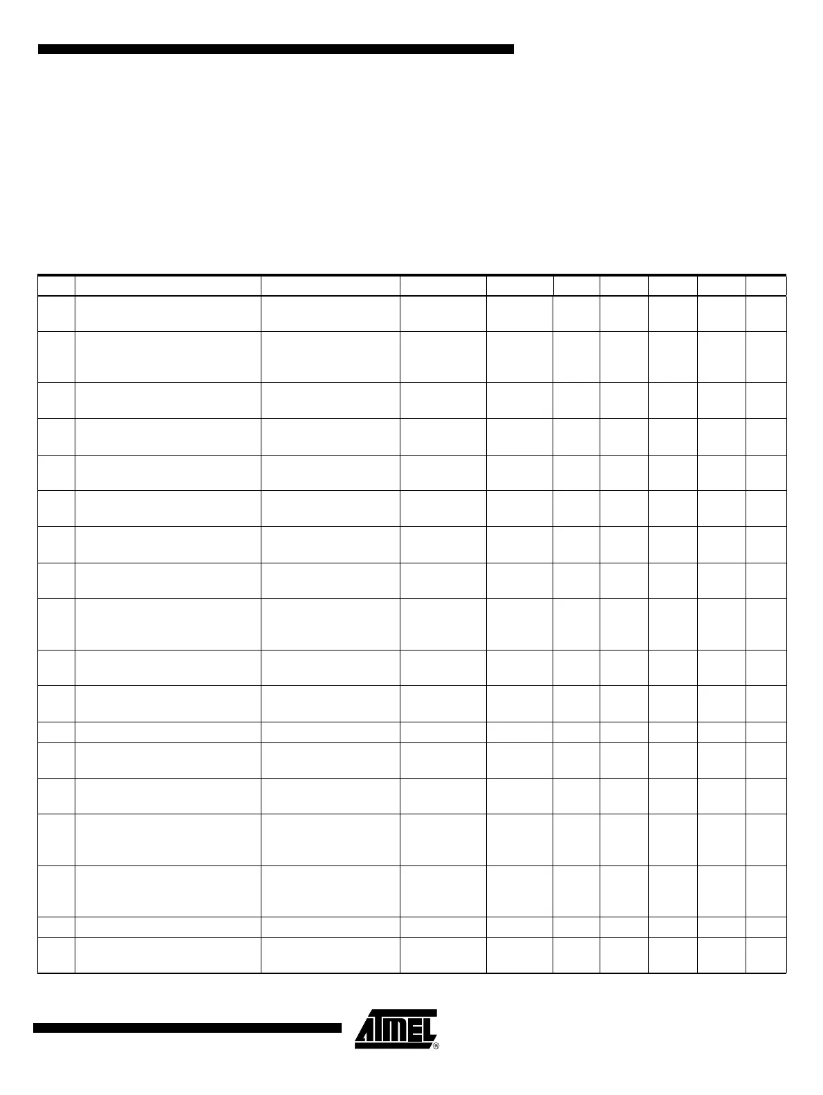
Table 9-1. Electrical Characteristics – EVZ Step-up Regulator
No. Parameters Test Conditions Pin Symbol Min Typ. Max. Unit Type*
8.1 Switching frequency
V
K30
≥ 8V or V
EVZ
≥ 8V
(after startup)
GEVZ f
GEVZ
–5% 100 +5% kHz A
8.2 Switching frequency
4V < V
K30
< 8V or
4V < V
EVZ
< 8V
(after startup)
GEVZ f
GEVZ
–10% 100 +10% kHz A
8.3
Voltage level at K15 to start the
EVZ regulator
See number 7.1 of
Table 8-2 on page 23
A
8.4
Hysteresis at K15 to stop the
EVZ regulator
See number 7.2 of
Table 8-2 on page 23
A
8.5
Voltage level at K30 to start the
EVZ regulator
See number 7.3 of
Table 8-2 on page 23
A
8.6
Hysteresis at K30 to stop the
EVZ regulator
See number 7.4 of
Table 8-2 on page 23
A
8.7
Voltage at pin GEVZ to switch
through the external driver
V
K30
≥ 3.85V to 5V
(ON threshold)
GEVZ V
GEVZ
V
K30
–
0.5V
V
K30
VA
8.8
Voltage at pin GEVZ to switch
through the external driver
V
K30
≥ 7V GEVZ V
GEVZ
610VA
8.9
Driving current at pin GEVZ to
switch through the external
driver
V
GEVZ
≤ 5V GEVZ I
GEVZ
–600 –80 mA A
8.10
Gate charge delivered to the
external FET
V
GEVZ
= 5V GEVZ Q
GEVZ
10 nC D
8.11
Gate charge delivered to the
external FET
V
GEVZ
= 10V GEVZ Q
GEVZ
20 nC D
8.12 Pull-down resistor at pin GEVZ GEVZ R
GEVZ
20 50 kΩ A
8.13
R
Dson
of dynamic sinking
transistor at GEVZ
GEVZ R
GEVZ
28 Ω A
8.15
Voltage between pins OCEVZ
and GND to detect overcurrent
OCEVZ V
OCEVZ
0.475 0.525 V A
8.16 Maximum switch duty cycle
V
K30
≥ 8V or V
EVZ
≥ 8V
(after startup)
V
EVZ
≥ 8V
GEVZ D
GEVZ
87.5 90 92.5 % A
8.17 Maximum switch duty cycle
4V < V
K30
< 8V or
4V < V
EVZ
< 8V
(after startup)
GEVZ D
GEVZ
75 90 92.5 % A
8.18 Minimum switch duty cycle GEVZ D
GEVZ
0%A
8.19
Overvoltage at pin EVZ to switch
off the regulator
V
EVZExt
programmed
(via external divider)
VEVZ V
EVZ
40.5 46.2 V A
*) Type means: A = 100% tested, B = 100% correlation tested, C = Characterized on samples, D = Design parameter