31
4929B–AUTO–01/07
ATA6264 [Preliminary]
Necessary for operation:
V
EVZ
= 5.5V to 40V, V
CP
> V
EVZ
+ 7V, V
INT
= 3.7V to 5.45V
Operating conditions of all other supply pins:
V
K30
, V
PERI
and V
CORE
are within functional range limits, T
j
= –40°C to +150°C
Other pins:
As defined in Section 4. ”Functional Range” on page 8.
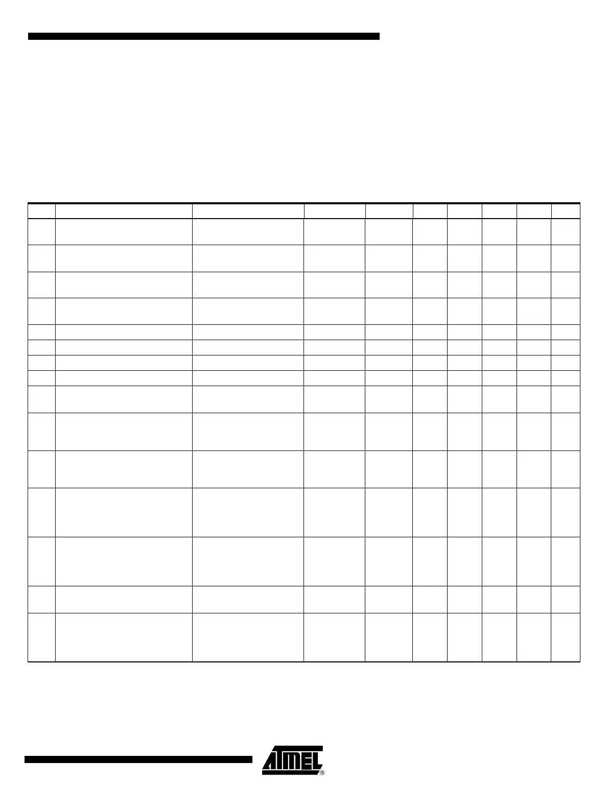
Table 10-1. Electrical Characteristics – VSAT Power Supply
No. Parameters Test Conditions Pin Symbol Min Typ. Max. Unit Type*
9.1
V
EVZ
voltage for the buck
converter to start running
EVZ V
EVZ
7.5 9 V A
9.2
V
EVZ
voltage for the buck
converter to stop
EVZ V
EVZ
5.5 6.2 V A
9.3
Regulator switch-on time via pin
EVZ
SVSAT t
SVSAT
020µsA
9.4
Regulator switch-off time via pin
EVZ
SVSAT t
SVSAT
05µsA
9.5 Regulator switching frequency V
EVZ
≥ 8V SVSAT f
SVSAT
–5% 200 +5% kHz A
9.5a Regulator switching frequency 5.5V > V
EVZ
≥ 8V SVSAT f
SVSAT
–10% 200 +10% kHz A
9.6 Output current limit SVSAT I
SVSAT
0.8 1 A A
9.7 R
Dson
of output transistor SVSAT R
SVSAT
1 Ω A
9.8
Output voltage #1 only at
V
PERI
=3.3V
Band-gap tolerance
included
VSAT V
VSAT1
–4% 7.8 +4% V A
9.9 Output voltage #2
V
VSAT2
programmed,
Band-gap tolerance
included
VSAT V
VSAT2
–4% 9.1 +4% V A
9.10 Output voltage #3
V
VSAT3
programmed,
Band-gap tolerance
included
VSAT V
VSAT3
–4% 10.4 +4% V A
9.11 Output transistor switch-on time
Time between reaching
0.1 × (V
EVZmax
– V
SVSATmin
)
and
0.9 × (V
EVZmax
– V
SVSATmin
)
150 ns A
9.12 Output transistor switch-on time
Time between reaching
0.9 × (V
EVZmax
– V
SVSATmin
)
and
0.1 × (V
EVZmax
– V
SVSATmin
)
150 ns A
9.13
Overvoltage switching off the
regulator
VSAT V
VSAT
1.1 ×
V
SATX
VA
9.14 Overvoltage switch-on time
Time between reaching
overvoltage and reaching
90% of V
SVSAT
maximum
under on condition
SVSAT t
SVSAToff
00.4µsA
*) Type means: A = 100% tested, B = 100% correlation tested, C = Characterized on samples, D = Design parameter
Notes: 1. Depending on implementation of slope compensation; sub-harmonics must be prevented
2. The value of the minimum load current must be higher than the internal pull-up current at pin VSAT to ensure proper func-
tion of the regulator