38
4929B–AUTO–01/07
ATA6264 [Preliminary]
11.25 Leading-edge blanking time t
blank
150 200 ns D
11.26
Slope of artificial ramp for
slope compensation
dV/dt 80
(1)
150
(1)
mV/µs D
11.27
Voltage level at K30 to switch
VCORE supply from EVZ to
K30 (V
VCORE
= 1.8V or 2.5V
programmed)
V
K30
increasing
See number 7.3 of Table
8-2 on page 23
A
11.28
Hysteresis at K30 to switch
VCORE supply from K30 to
EVZ
(V
VCORE
= 1.8V or 2.5V
programmed)
V
K30
decreasing
See number 7.4 of Table
8-2 on page 23
A
11.29
Voltage level at K30 to switch
VCORE supply from EVZ to
K30 (V
VCORE
= 5V
programmed)
V
K30
increasing K30 V
K30
6.1 8.1 V A
11.30
Hysteresis at K30 to switch
VCORE supply from K30 to
EVZ (V
VCORE
= 5V
programmed)
V
K30
decreasing K30 V
K30
0.5 1 V A
11.31
Time to switch VCORE
supply from EVZ to K30 or
K30 to EVZ
SVCORE t
switch
07.6µsD
11.32
VCORE loss-detection
threshold
(2)
VCORE I
Load
01mAD
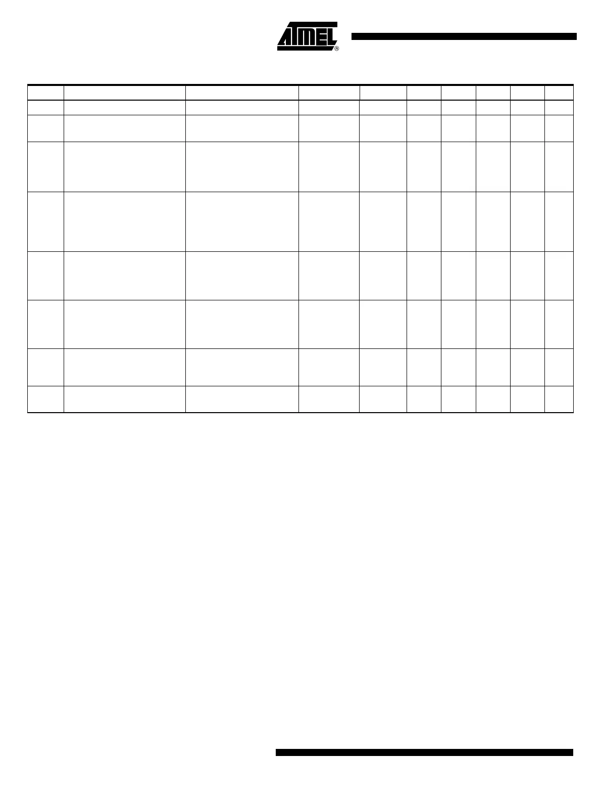
Table 12-1. Electrical Characteristics (Continued)– VCORE Power Supply
No. Parameters Test Conditions Pin Symbol Min Typ. Max. Unit Type*
*) Type means: A = 100% tested, B = 100% correlation tested, C = Characterized on samples, D = Design parameter
Notes: 1. Depending on implementation of slope compensation, sub-harmonics have to be prevented.
2. The value of the minimum load current must be higher than the internal pull-up current at pin VCORE to ensure proper
function of the regulator.