46
4929B–AUTO–01/07
ATA6264 [Preliminary]
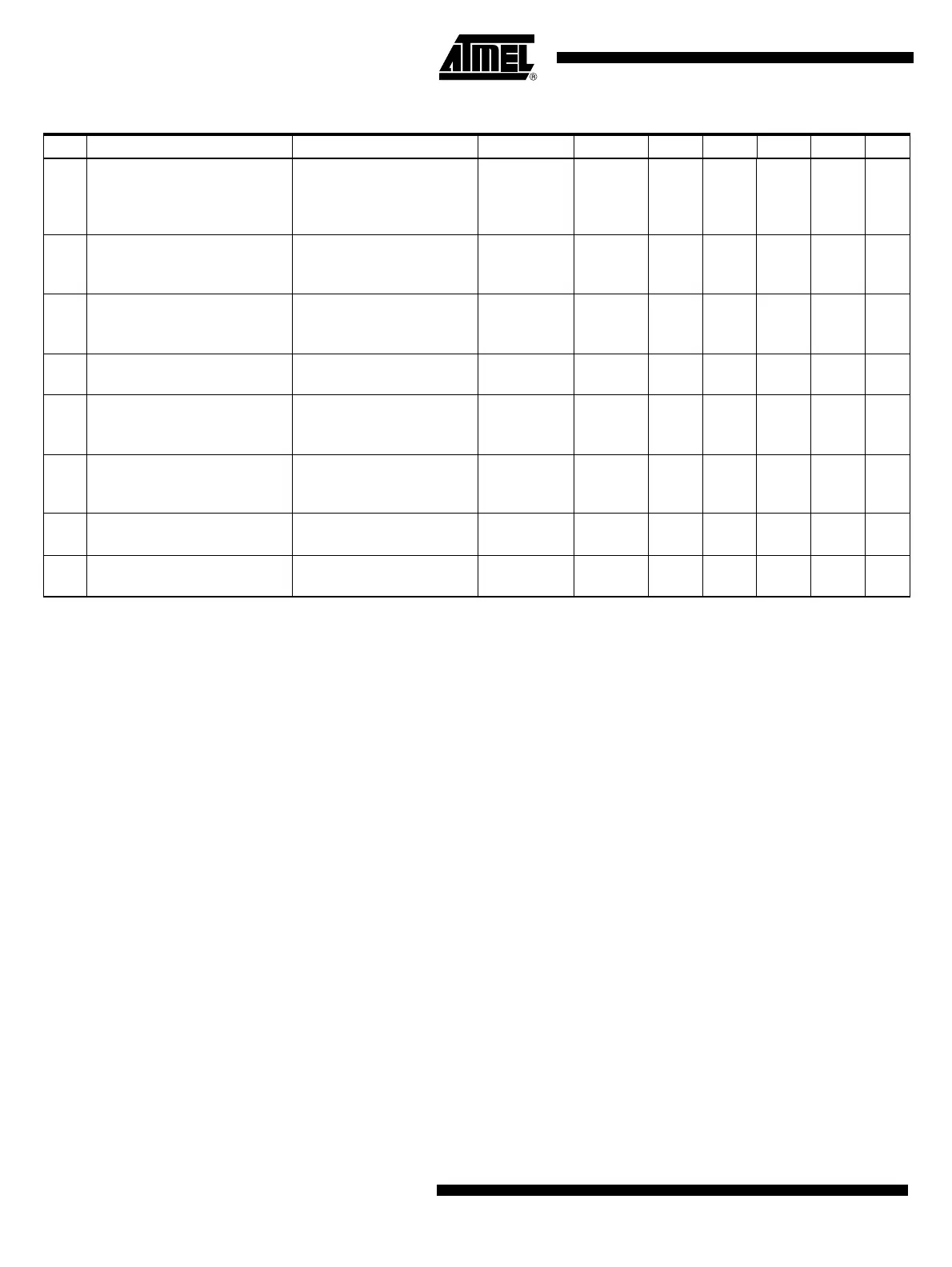
14.15
Delay time for RESQ and
RESQ2 to switch to low after
reaching the reset threshold of
V
EVZ
RESQ
RESQ2
t
RESQ
t
RESQ2
10 20 µs A
14.16 Pull-down current at pin RESQ
RESQ is switched to low
(V
RESQ
= 0.4V),
1V ≤ V
VPERI
<5.5V
RESQ I
RESQ
12mAA
14.17
Pull-down current at pin
RESQ2
RESQ2 is switched to low
(V
RESQ
= 0.4V),
1V ≤ V
VPERI
<5.5V
RESQ2 I
RESQ2
12mAA
14.18
Pull-down resistor at pin
RESQ, RESQ2
RESQ
RESQ2
R
RESQ
R
RESQ2
0.5 1.5 MΩ D
14.19
Output current high side
RESQ, RESQ2
RESQ, RESQ2 are
switched to high,
V
RESQ
, V
RESQ2
= 0V
RESQ
RESQ2
I
RESQ
I
RESQ2
–550 –250 µA A
14.20
Output current low side RESQ,
RESQ2
RESQ, RESQ2 are
switched to high,
V
RESQ
, V
RESQ2
= V
VPERI
RESQ
RESQ2
I
RESQ
I
RESQ2
410mAA
14.21 Rise time RESQ, RESQ2
30-pF external capacitive
load
RESQ
RESQ2
t
RESQ
t
RESQ2
4.0 µs A
14.22 Fall time RESQ, RESQ2
30-pF external capacitive
load
RESQ
RESQ2
t
RESQ
t
RESQ2
0.5 µs A
Table 15-2. Electrical Characteristics (Continued)– Reset Function (Pin RESQ and Pin RESQ2)
No. Parameters Test Conditions Pin Symbol Min Typ. Max. Unit Type*
*) Type means: A = 100% tested, B = 100% correlation tested, C = Characterized on samples, D = Design parameter
 Loading...