— 6 —
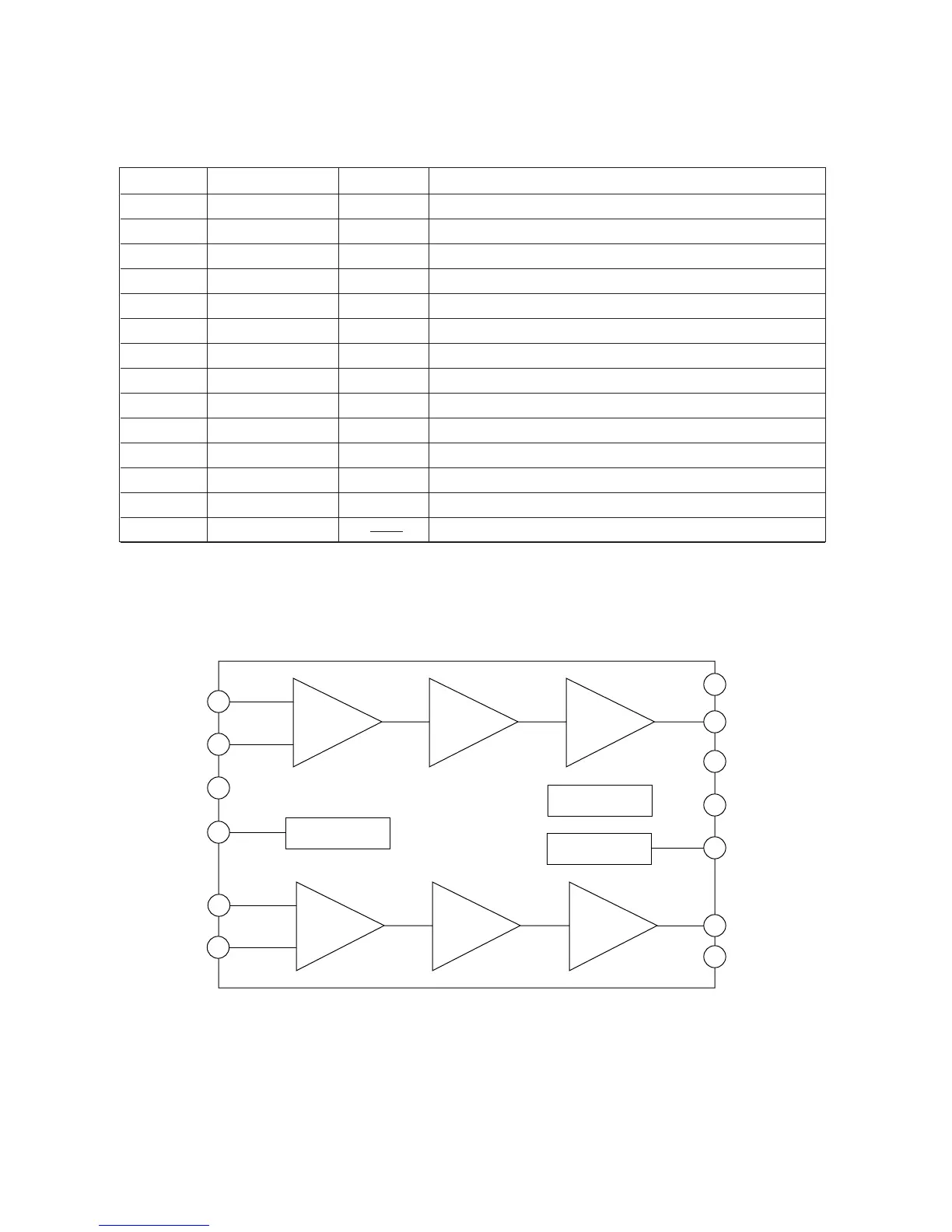
Pin No. Terminal In/Out Functiion
1 Power GND In Ground (0 V) source
2 Ch1 B.S. Out Terminal for a bootstrap capacitor
3 Ch1 OUT Out Channel1 output
4 VCC In +9 V source. Connected to the power source directly.
5 Ch1 N.F. In Negative feedback input
6 Ch1 IN In Channel1 input
7 D.C. Out Terminal for a decoupling capacitor
8 Pre GND In Ground (0 V) source
9 Standby In Power control signal input. 0 V: OFF, +9 V: ON
10 Ch2 IN In Channel2 input
11 Ch2 N.F. In Negative feedback input
12 Ch2 OUT Out Channel2 output
13 Ch2 B.S. Out Terminal for a bootstrap capacitor
14 NC Not used.
POWER AMPLIFIER (IC101: LA4598)
The following table shows the pin functions of IC101.
6
5
8
7
10
11
13
12
9
4
1
3
2
Input
Amp.
Pre-drive
Amp.
Power
Amp.
TSD protector
Stand by
Bias circuit
Input
Amp.
Pre-drive
Amp.
Power
Amp.
Ch1 IN
Ch1 N.F.
Pre GND
D.C.
Ch2 IN
Ch2 N.F.
Ch2 B.S.
Ch1 OUT
Power GND
VCC
Standby
Ch2 OUT
Ch2 B.S.
Internal Block Diagram of IC101
 Loading...