— 17 —
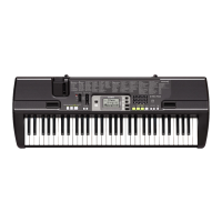
KEY TOUCH LSI (LSI10: TC190C020AF-001)
By counting the time between first-key input signal FI and second-key SI from the keyboard unit, the key
touch LSI detects key velocity of 256-step. Then the LSI sends the CPU the note number and its velocity
data.
Pin No. Terminal In/Out Function
1 WRB In Write signal from CPU.
2 ~ 11, 13,
D0 ~ D15 In/Out Data bus.
14, 16 ~ 19
12 VSS In Ground terminal (0 V).
15 VDD In VDD (5 V) source.
20 ~ 23 CA0 ~ CA3 In Address bus.
24 VSS In Ground terminal (0 V).
25 ~ 32, FI0 ~ FI4,
In Key input signal.
34, 35 SI0 ~ SI4
33 VDD In VDD (5 V) source.
36 ~ 38,
KC0 ~ KC7 Out Key scan signal.
40 ~ 44
39 VSS In Ground terminal (0 V).
45 VDD In VDD (5 V) source.
46 ~ 51
FI5 ~ FI7
In Key input signal.
SI5 ~ SI7
52 VSS In Ground terminal (0 V).
53 ~ 58,
FI8 ~ FI10
60 ~ 62
SI8 ~ SI10 In Key input signal (Not used).
KI0 ~ KI2
59 VDD In VDD (5 V) source.
63, 64
MODE0, MODE1
— Not used.
65 VSS In Ground terminal (0 V).
66 KCKI In Clock signal for key common/input.
67 ~ 72,
— Not used.
74 ~ 77
73 VDD In VDD (5 V) source.
78 RESB In Reset signal from CPU.
79 CSB In Chip selection signal.
80 RDB In Read signal from CPU.
 Loading...