— 12 —
Pin No. Terminal In/Out Function
106 EOEB Out Read enable signal output for the effect RAM
108 VCC7 In +5V source
111 ECEB Out Chip select signal output for the effect RAM
113 ~ 117 ED11 ~ ED15 — Not used
118 VCC4 In +5V source
119 GND4 In Ground (0V) source
120 ~ 122 ED8 ~ ED10 — Not sued
123 ~ 130 ED0 ~ ED7 In/Out Data bus for the effect RAM
131 GND5 In Ground (0V) source
132 ~ 134 — — Not used. Connected to ground.
135, 136 — — Not used
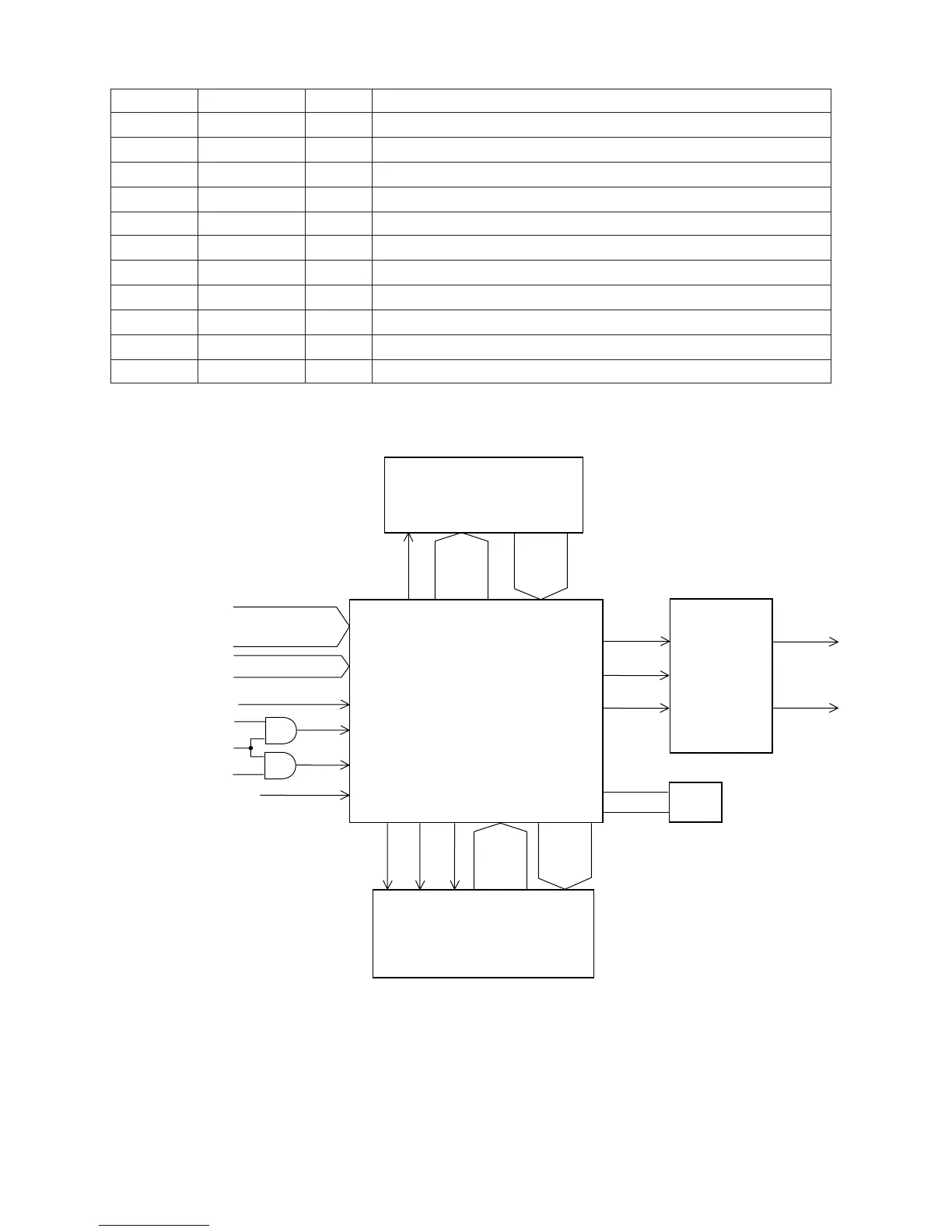
Block diagram of DSP and DAC circuit
DAC (LSI101: UPD6376GS)
The DAC receives 16-bit serial data and two clocks output from the DSP. The DAC converts the data into
analog waveforms by each channel and output them separately.
The following table shows the pin functions of LSI101.
DSP
LSI103
HG51B155FD-1
Effect RAM (256K-bit)
LSI102
LC33832M-70
Sound Source ROM
LSI105
TC5316200CF-C117
CE
A0 ~ A19 D0 ~ D15
RA0 ~
RA19
RD0 ~
RD15
RA22
D0 ~ D7
A0 ~ A3
A13
SOLP
BOK
WOK1
EA0 ~
EA14
ED0 ~
ED15
CS
WE
OE
D0 ~ D15
A0 ~ A14
ECEB EOEB
EWEB
PG
X102
24.576 MHz
DAC
LSI101
UPD6376GS
LOUT
ROUT
SOLP: Sound data
BOK: Bit clock
WOK1: Word clock
SI
CLK
LRCK
RD
WR
RESET
Power ON signal
CCSB
CRDB
CWRB
RESB
 Loading...