— 11 —
OFF
ON
SWO
SW
CPU
MAIN SWITCH
VDD
"L"
"L"
KAC
KIO
(Pin36)
(Pin62)
(Pin54)
(Pin53)
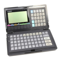
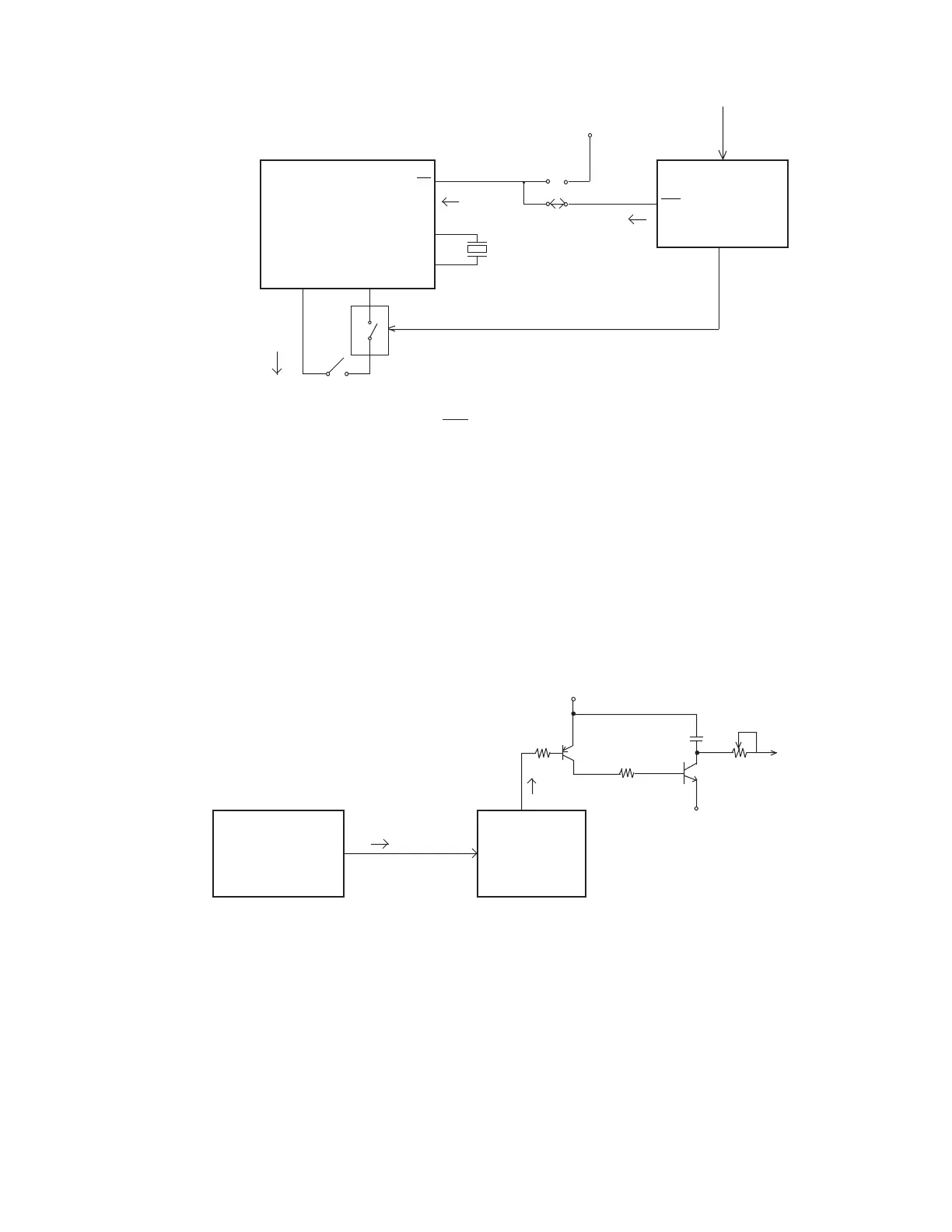
5) Main switch and power on switch
When the main switch is set to on position, SW terminal of CPU receives "L", then KAC terminal will be
"L" to enable the system power on. The KI0 terminal is "H" when VDD is applied to CPU. Therefore,
when pressing the power on switch, CPU will generate a clock pulse (2 MHz) at OSCO terminal for
start up the system.
When the PDN terminal will be receiving "L" level, GATE ARRAY will send "L" signal from KON termi-
nal for cutting the line of power on switch.
HD62076C03
from IC4
(Pin35)
VOB
VIN
"L"
V2ON
CPU
GND
(Pin45) (Pin24)
(Pin28) (Pin31)
When the system is start up, CPU will send "H" signal to VIN terminal of gate array from V2ON termi-
nal. Then, gate array will send "L" signal from VOB terminal to turn ON the transistors Q2 and Q1 for
LCD drive voltages.
HD62076C03
"H"
GATE ARRAY
(Pin2)
(Pin1)
R3
R2
VR1
VDD
C20
V1~V4
(Pin3)
6) Power supply for LCD
PDN
GATE ARRAY
KON
(Pin26)
(Pin3)
"L"
"H"
POWER ON SWITCH
4S66F
OSCO
OSCI
2 MHz
 Loading...