-7-
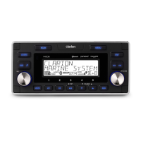
CX501/CX501B/CX501A
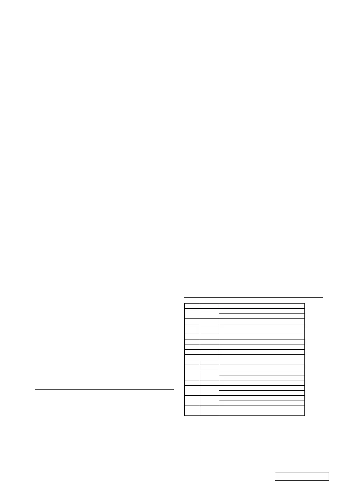
051-3730-00 LV5680P
Power IC
Pin No. Terminal Function
ILM OUT At CTRL1=M1,M2,H,
OUT=ON 12.0V/300mA
2
ILM_F
ILM Feed back
CD OUT At CTRL2=M,H,
OUT=ON 12.0V/300mA
4
AUDIO_F
AUIDO Feed back
5
AUDIO
AUDIO OUT At CTRL2=M,H,ǂǂOUT=ON
6
CTRL2
CTRL2(Input) 3 Values input
7
VCC
Power
8
CTRL1
CTRL1(Input) 4 Values input
9
GND
GND
10
ACC
Accessory detector(input)
Accessory OUT
At ACC˚3V, OUT=ON
12
VDD5V
VDD5V OUT 5.0V/500mA
SW5V OUT
At CTRL2=M,H, OUT=ON
ANT OUT At CTRL1=H, OUT=ON
VCC-0.5V/300mA
EXT OUT At CTRL1=M2,H,
OUT=ON VCC-0.5V/350mA
ILM
1
CD3
ACC5V
EXT
15
13
ANT
11
SW5V
14
pin 43 : GP50 : I/O : General purpose I/O port with pull down resistor.
pin 44 : GP51 : I/O : General purpose I/O port with pull down resistor.
pin 45 : GP52 : I/O : General purpose I/O port with pull down resistor.
pin 46 : GP53 : I/O : General purpose I/O port with pull down resistor.
pin 47 : GP30 : I/O : General purpose I/O port with pull down resistor.
pin 48 : GP31
: I/O : General purpose I/O port with pull down resistor.
pin 49 : GP32 : I/O : General purpose I/O port with pull down resistor.
pin 50 : GP33 : I/O : General purpose I/O port with pull down resistor.
pin 51 : GP34
: I/O : General purpose I/O port with pull down resistor.
pin 52 : GP35
: I/O : General purpose I/O port with pull down resistor.
pin 53 : GP36
: I/O : General purpose I/O port with pull down resistor.
pin 54 : GP37 : I/O : General purpose I/O port with pull down resistor.
pin 55 : MODE0 :
IN
: LSI mode set pin 0 This pin must be .
connected to the 0V level.
pin 56 : MODE1 :
IN
: LSI mode set pin 1 This pin must be connected
to the 0V level.
pin 57 : DVDD
: - : Digital system power supply.
pin 58 : DVSS
: - : Digital system ground. This pin must be
connected to the 0V level.
pin 59 : RESB :
IN
: IC reset input ("L"-active).
pin 60 : SIFCK :
IN
: Host-I/F.
pin 61 : SIFDI :
IN
: Host-I/F.
pin 62 : SIFDO
:
IN
: Host-I/F.
pin 63 : SIFCE :
IN
: Host -I/F.
pin 64 : BUSYB
:
IN
: Host -I/F.
pin 65 : GP03
: I/O : General purpose I/O port with pull down resistor.
pin 66 : GP04 : I/O : General purpose I/O port with pull down resistor.
pin 67 : GP05
: I/O : General purpose I/O port with pull down resistor.
pin 68 : GP06
: I/O : General purpose I/O port with pull down resistor.
pin 69 : GP07
: I/O : General purpose I/O port with pull down resistor.
pin 70 : XVDD1
: - : Oscillator power supply.
in 71 : XIN :
IN
: 12MHz oscillator connection.
pin 72 : XOUT : O : 12MHz oscillator connection.
pin 73 : XVSS1
: - : Oscillator ground.
This pin must be connected to the 0V level.
in 74 : UDM : I/O : USB data in
ut/out
ut Dˉ si
nal connection.
in 75 : UDP : I/O : USB data in
ut/out
ut Dˇ si
nal connection.
pin 76 : UVDD : - : USB power supply.
pin 77 : VVDD2
: - : System PLL power supply.
in 78 : VVSS2 : - : S
stem PLL
round.
This
in must be connected to the 0V level.
pin 79 : AFILT : - : Audio PLL charge pump output.
pin 80 : VVDD3
: - : Audio PLL power supply.
in 81 : MODE2 :
IN
: LSI mode set
in2.
This
in must be connected to the 0V level.
in 82 : JTRSTB :
IN
:JTAGresetin
ut .
in 83 : JTCK :
IN
: JTAG clock in
ut .
pin 84 : JTDI :
IN
: JTAG data input .
pin 85 : JTMS
:
IN
: JTAG mode input.
pin 86 : JTDO
: O : JTAG data output.
in 87 : JTRTCK : O : JTAG return clock out
ut .
pin 88 : DVDD : - : Digital system power supply.
pin 89 : DVSS
: - : Digital system ground.
This pin must be connected to the 0V level.
in 90 : DVDD15 :
IN
:Ca
acitor connection
in for internal re
ulator.
pin 91 : XVSS2 : - : Oscillator ground.
This pin must be connected to the 0V level.
pin 92 : X16OUT
: O : 16.9344MHz oscillator connection.
in 93 : X16IN :
IN
: 16.9344MHz oscillator connection.
in 94 : XVDD2 : - : Oscillator
ower su
l
.
pin 95 : LRVDD : - : Audio LPF power supply.
pin 96 : LCHO
: O : Audio Lch data output.
in 97 : LRREF :
IN
: Reference volta
e for audio LPF.
in 98 : RCHO : O : Audio Rch data out
ut.
pin 99 : LRVSS : - : Audio LPF ground.
This pin must be connected to the 0V level.
in 100 : SLCO : O : Slice Level Control out
ut.
1.Terminal Description
pin 1
:
SPK_A_N
:O
:
Speaker output negative (left side).
pin 2
:
SPK_A_P
:O
:
Speaker output positive (left side).
pin 3
:
SPK_B_N
:O
:
Speaker output negative (right side).
pin 4
:
SPK_B_P
:O
:
Speaker output positive (right side).
pin 5
:
GND
:-
:
Ground.
pin 6
:
MIC_A_P
:IN
:
Microphone input positive (left side).
pin 7 : MIC_A_N :
IN
: Microphone input negative (left side).
pin 8
:
MIC_B_P
:IN
:
Microphone input positive (right side).
pin 9 : MIC_B_N :
IN
: Microphone input negative (right side).
pin 10
:
NC
:IN
:
Not in use.
pin 11
:
PCM_IN
:IN
:
Synchronous data input.
pin 12 : PCM_SYNC :
-
: Synchronous data sync.
pin 13 : PCM_CLK :
-
: Synchronous data clock.
060-8123-90 GTBM501 Bluetooth System controller
pin 14 : PCM_OUT :
O
: Synchronous data output.
pin 15 AIO0 I/O Analogue programmable input/output line.
pin 16
:
AIO1
:
I/O
:
Analogue programmable input/output line.
pin 17
:
PIO12
:
I/O
:
Programmable input/output line.
pin 18
: GND : - : Ground.
pin 19
:POWER :
O
: +3.3V Supply
pin 20
: USB_DP : I/O : USB data plus with selectable internal
1.5kಳ pull-up resistor
pin 21
: USB_DN : : USB data minus.
pin 22
:
UART_RTS
:O:
UART request to send active low.
pin 23
:
UART_CTS
:O:
UART clear to send active low.
pin 24
:
UART_TX
:O:
UART data output.
pin 25
:UARTR_RX :
IN
: UART data input.
pin 26
: RESET : O : Reset If Low.
pin 27
: GND : - : Ground.
pin 28
: PIO4 : I/O : Programmable input/output line.
pin 29
:
PIO5
:
I/O
:
Programmable input/output line.
pin 30
: PIO6 : I/O : Programmable input/output line.
pin 31
: PIO7 : I/O : Programmable input/output line.
pin 32
:
SPI_MOSI
:IN:
SPI data input.
pin 33
: SPI_CSB : O : Chip select for SPI, active low.
pin 34
: SPI_CLK : O : SPI clock.
pin 35
: SPI_MISO : O : SPI data output.
pin 36
: PIO10 : I/O : Programmable input/output line.
pin 37
: PIO11 : I/O : Programmable input/output line.
pin 38
:
PIO3
:
I/O
:
Programmable input/output line.
pin 39
: PIO2 : I/O : Programmable input/output line.
pin 40
: PIO1 : I/O : Programmable input/output line.
pin 41
: PIO0 : I/O : Programmable input/output line(external RXEN).
pin 42
:
PIO8
:
I/O
:
Programmable input/output line.
pin 43
: PIO9 : I/O : Programmable input/output line.
pin 44
: GND : - : Ground.
pin 45
: AUX_DAC : O : 8-bit voltage output DAC.
pin 46
:
GND
:
-
:
Ground.
pin 47
:ANT :
IN
: RF Interface.
pin 48
: GND : - : Ground.
pin 49
:
GND
:
-
:
Ground.
pin 50
: VBUS :
IN
: Lithium ion/polymer battery charger input.
pin 51
: VBATT : O : Lithium ion/polymer battery positive
terminal. Battery charger output and
input to switch-mode regulator.
pin 52
: GND : - : Ground.
pin 53
: MIC_BIAS : O : 2.7V/Programmable Mic Bias Output.
 Loading...